Display device and method of measuring contact resistance thereof

a technology of display device and contact resistance, which is applied in the field of display device and a method of measuring contact resistance thereof, can solve the problem of insufficient space for disposing a dummy pad for resistance measuremen

Active Publication Date: 2017-03-23
LG DISPLAY CO LTD
View PDF4 Cites 11 Cited by
  • Summary
  • Abstract
  • Description
  • Claims
  • Application Information

AI Technical Summary

Benefits of technology

[0019]An aspect of the present disclosure provides a display device in which bonding resistance is automatically measured without having to dispose a separate dummy pad in a display panel, and a method for measuring contact resistance of a driving circuit thereof.

Problems solved by technology

First, since the dummy pad formed on the substrate of the display panel to manually measure bonding resistance is exposed, static electricity may be introduced through the dummy pad. Static electricity may be introduced to a line or transistor for auto-probe inspection to damage the element.
Second, static electric may be charged through the dummy pad during an alignment film rubbing process and the charged static electricity is discharged to a neighbor signal line or transistor during a follow-up process to damage the element.
Third, a wearable device such as a smart watch or a dashboard of a vehicle has a narrow bezel, and thus, a space for disposing a dummy pad for resistance measurement is insufficient. Various forms of curved design are applied to display panels.

Method used


Image

  • Display device and method of measuring contact resistance thereof
  • Display device and method of measuring contact resistance thereof
  • Display device and method of measuring contact resistance thereof

Examples


Embodiment Construction

[0032]Hereinafter, embodiments of the present disclosure will be described in detail with reference to the accompanying drawings. Like reference numerals refer to like elements throughout. In describing the present disclosure, if a detailed explanation for a related known function or construction is considered to unnecessarily divert the gist of the present disclosure, such explanation will be omitted but would be understood by those skilled in the art.

[0033]A display device of the present disclosure may be implemented as a liquid crystal display (LCD), a field emission display (FED), a plasma display panel (PDP), an organic light emitting display device, an electrophoresis display (EPD), and the like. In the following embodiment, an LCD device will be largely described as an example of a flat panel display, but the present disclosure is not limited thereto. For example, the present disclosure may be applied to any display device requiring auto-probe inspection.

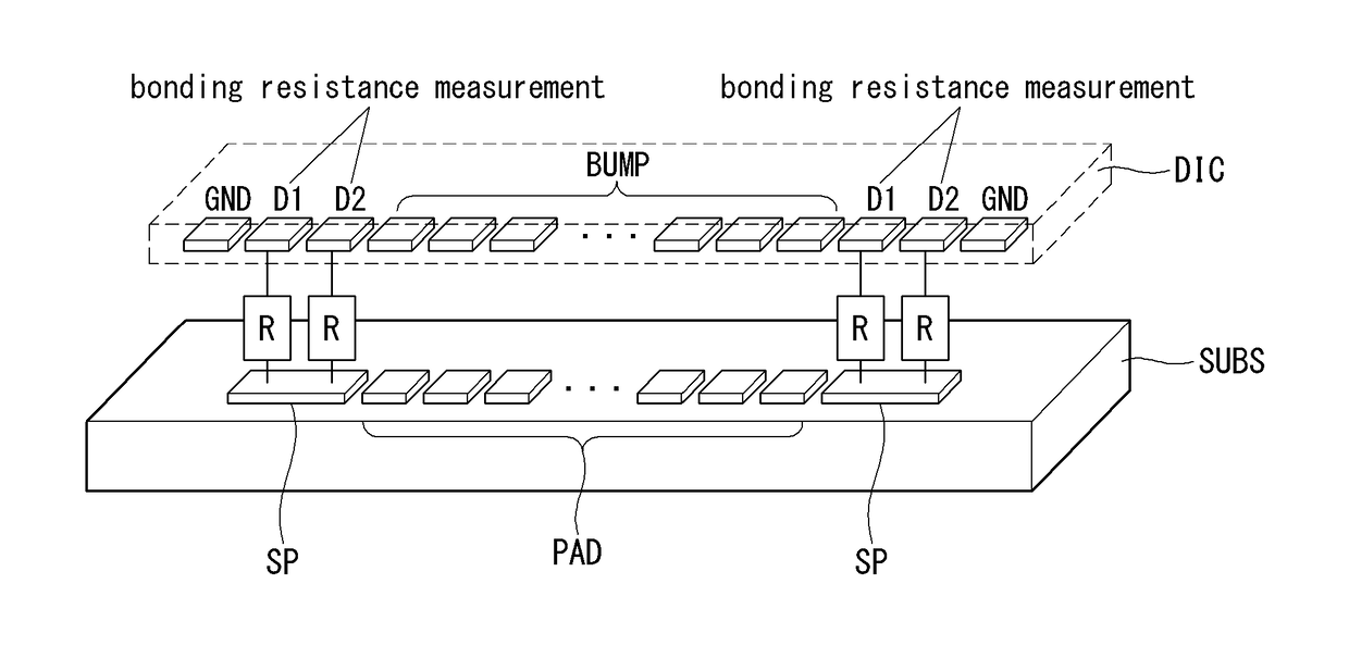
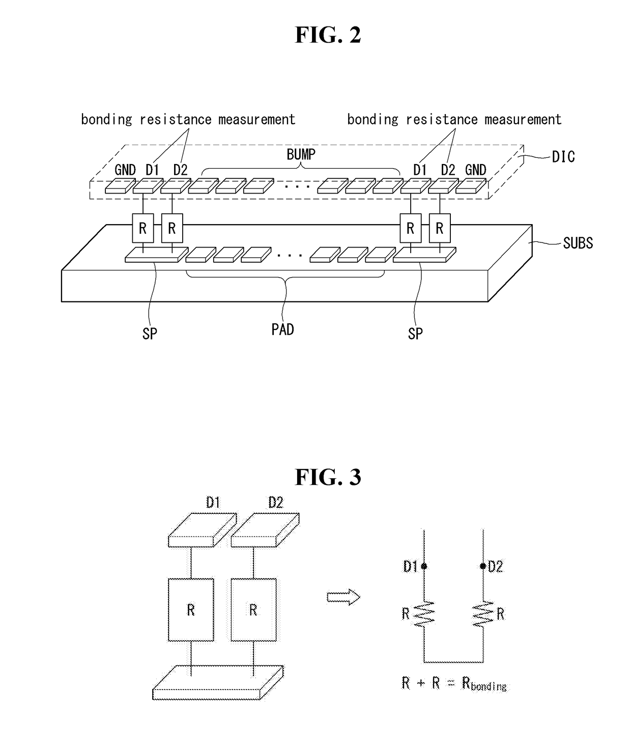
[0034]Referring to FI...


PUM


Abstract

Provided are a display device and a method for measuring contact resistance thereof. A plurality of dummy bumps disposed on a driving circuit or a flexible circuit board are connected to shorting pads disposed on the display panel, and bonding resistance is measured by comparing an input voltage of a comparator input through bonding resistance between dummy bumps and shorting pads with a variable reference voltage.

Description

[0001]This application claims the benefit of Korean Patent Application No. 10-2015-0131843 filed on Sep. 17, 2015, the entire contents of which is incorporated herein by reference for all purposes as if fully set forth herein.BACKGROUND OF THE INVENTION[0002]Field of the Invention[0003]The present disclosure relates to a display device and a method for measuring contact resistance thereof.[0004]Discussion of the Related Art[0005]Various flat panel display devices such as a liquid crystal display (LCD), an organic light emitting display device, a plasma display panel (PDP), an electrophoretic display (EPD), and the like, have been developed.[0006]An LCD displays an image by controlling an electric field applied to liquid crystal molecules according to a data voltage. An active matrix type LCD has thin film transistors (TFTs) formed in every pixel.[0007]A process of manufacturing an LCD includes a substrate cleaning process, a substrate patterning process, an alignment film forming / ru...

Claims


Application Information

Patent Timeline
Patent Type & Authority Applications(United States)
IPC IPC(8): G06F3/045G06F3/041
CPCG06F3/0412G06F3/045G01R27/20G02F1/13306G02F1/13458G09G3/006G02F1/133G02F1/1309G02F1/13454G06F11/2221
Inventor KANG, JEONGHO
Owner LG DISPLAY CO LTD
Why Eureka
Try Eureka