Temperature measuring device for semiconductor manufacturing apparatus, method of measuring temperature in semiconductor manufacturing apparatus, and semiconductor manufacturing apparatus

Inactive Publication Date: 2007-12-13
FUJITSU SEMICON LTD
View PDF3 Cites 9 Cited by
  • Summary
  • Abstract
  • Description
  • Claims
  • Application Information

AI Technical Summary

Benefits of technology

[0020]The semiconductor manufacturing apparatus is provided with the fastening device for fixing the temperature measuring device which is provided with the temperature sensor, on the wafer mounting portion. Moreover, the apparatus is configured in a way that an output of the temperature sensor of the temperature measuring device is taken out to the outside via the fastening device. Accordingly, an opera

Problems solved by technology

For example, in the chemical vapor deposition (CVD) process at the time of forming a film, large unevenness is caused in the film thickness if the temperature of the wafer is not strictly managed.
In addition, in the etching process at the time of forming a wiring, a defect, such as an increase in the wiring resistance, a short circuit, or disconnection, is caused if the temperature of the wafer is not strictly managed.
However, in an apparatus of this kind, temperature on a wafer surface is not directly measured.
For this reason, the temperature is not managed at a sufficiently strict level.
In addition, the thermocouple arranged in the apparatus cannot measure the distribution of the temperature

Method used


Image

  • Temperature measuring device for semiconductor manufacturing apparatus, method of measuring temperature in semiconductor manufacturing apparatus, and semiconductor manufacturing apparatus
  • Temperature measuring device for semiconductor manufacturing apparatus, method of measuring temperature in semiconductor manufacturing apparatus, and semiconductor manufacturing apparatus
  • Temperature measuring device for semiconductor manufacturing apparatus, method of measuring temperature in semiconductor manufacturing apparatus, and semiconductor manufacturing apparatus

Examples


Embodiment Construction

[0028]Descriptions will be provided below by referring to the accompanying drawings.

(Temperature Measuring Device)

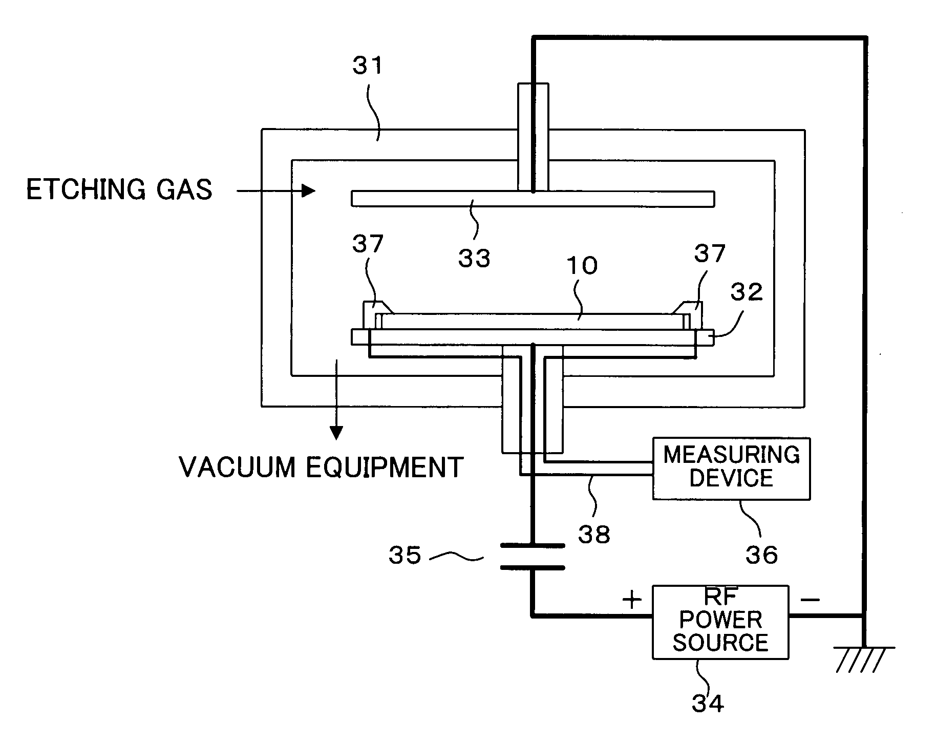
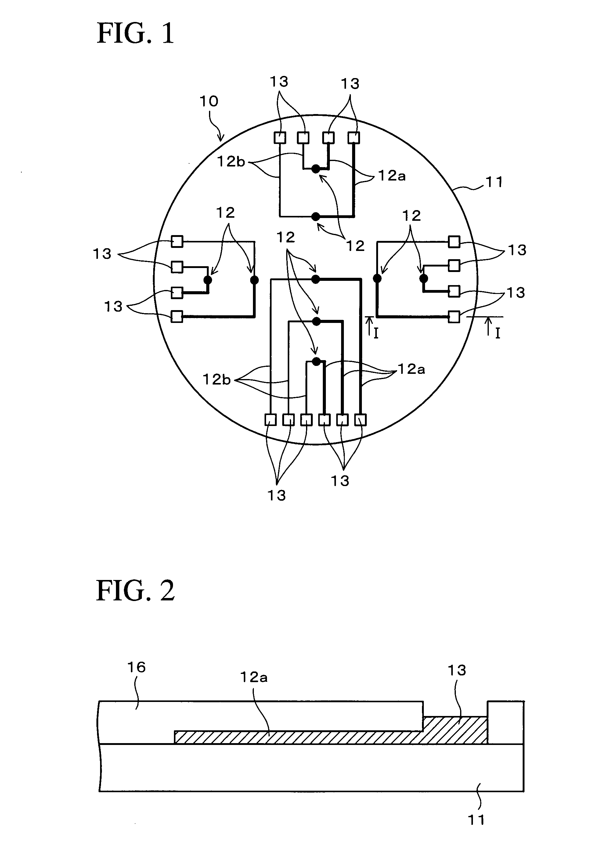
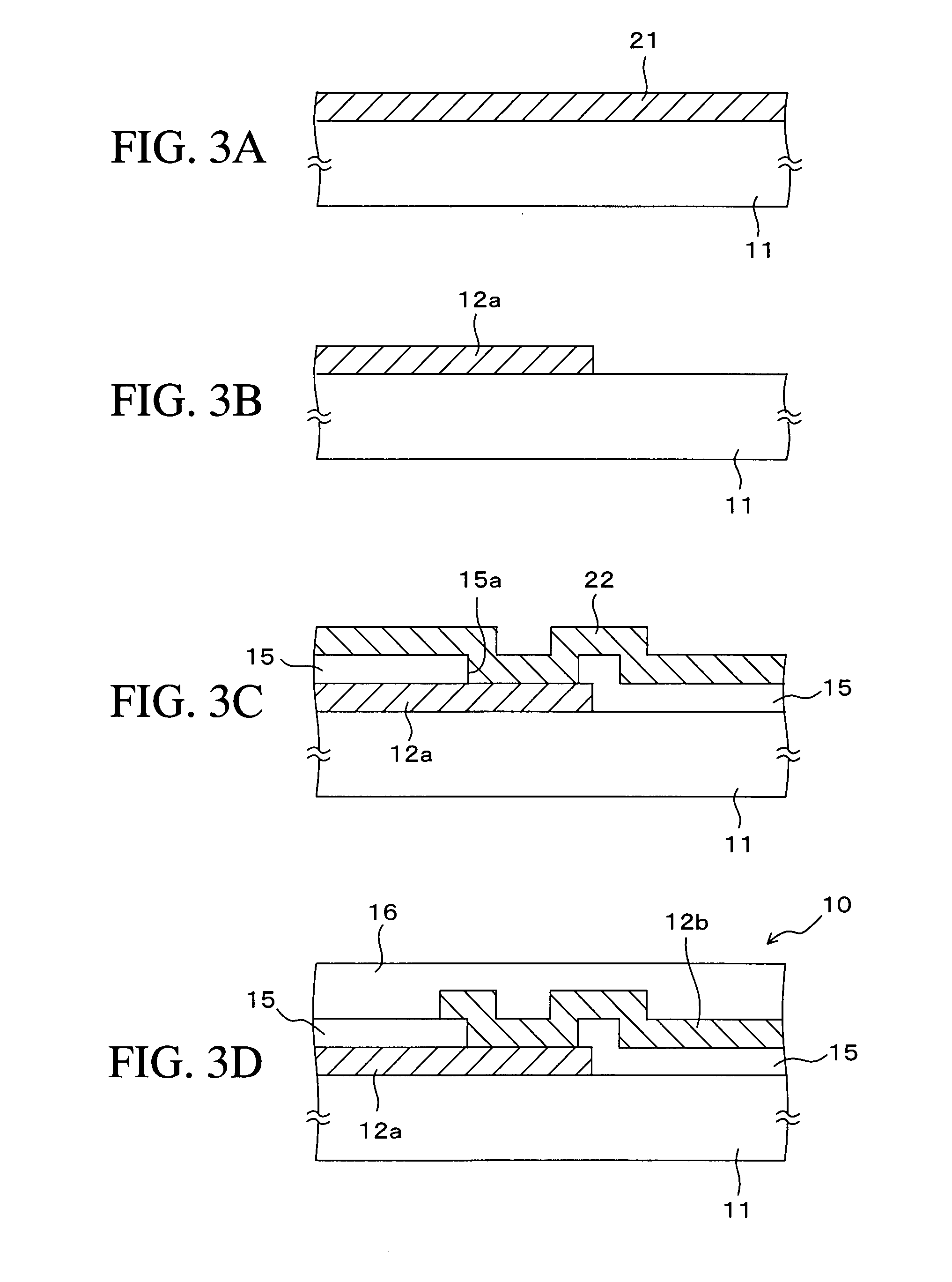
[0029]FIG. 1 is a schematic plan view showing a temperature measuring device for a semiconductor manufacturing apparatus according to an embodiment. FIG. 2 is a schematic cross-sectional view in a position shown by the I-I line in FIG. 1.

[0030]A temperature measuring device 10 for a semiconductor manufacturing apparatus according to the present embodiment is configured of a substrate 11 and a plurality of thermocouples (temperature sensors) 12 formed on the substrate 11. Each of these thermocouples 12 are formed in such a manner that one of tip ends of each of two metal wires 12a and 12b are jointed together, the materials of the respective metal wires 12a and 12b being mutually different. Each of portions (shown by black dots in FIG. 1) where the metal wires 12a and 12b are joined together is termed as a temperature measuring junction where a voltage corresponding to a ...


PUM


Abstract

A temperature measuring device is configured of a substrate formed of a silicon wafer, a thermocouple formed by using the film forming method, the photolithographic method, and the etching method, and a clamp pad (an electrode pad) which is arranged in an edge portion of the substrate, and which is connected to the thermocouple. In a semiconductor manufacturing apparatus, the temperature measuring device is fixed on a wafer mounting portion with a clamper pin (a fastening device) being in contact with the clamp pad. An output of the thermocouple is taken out to the outside through the clamper pin.

Description

CROSS-REFERENCE TO RELATED APPLICATIONS[0001]This application is based on and claims priority of Japanese Patent Application No. 2006-158024 filed on Jun. 7, 2006, the entire contents of which are incorporated herein by reference.BACKGROUND OF THE INVENTION[0002]1. Field of the Invention[0003]It is related to a temperature measuring device for a semiconductor manufacturing apparatus, which measures the temperature of a semiconductor wafer in a process of manufacturing a semiconductor device (an LSI: a large scale integrated circuit); a method of measuring temperature, by using the temperature measuring device, in the semiconductor manufacturing apparatus; and a semiconductor manufacturing apparatus which measures temperature by using the temperature measuring device.[0004]2. Description of the Prior Art[0005]In processing for manufacturing a semiconductor device (an LSI), there are a number of processes for heating a semiconductor wafer, such as a film forming process, an impurity d...

Claims


Application Information

Patent Timeline
IPC IPC(8): G01K1/14G01K7/00
CPCG01K7/028G01K1/146
Inventor TOYOSHIMA, YOSHITAKA
Owner FUJITSU SEMICON LTD
Why Eureka
Try Eureka