
Imprint mold and imprint method

a technology of imprinting mold and imprinting method, which is applied in the field of imprinting mold, can solve the problems of difficult reuse of damaged molds, increased mold manufacturing cost, and long time to complete, and achieve the effects of accurate detection of magnitude, control of pattern accuracy, and high accuracy

Active Publication Date: 2017-04-20
DAI NIPPON PRINTING CO LTD
View PDF2 Cites 1 Cited by
  • Summary
  • Abstract
  • Description
  • Claims
  • Application Information

AI Technical Summary

Benefits of technology

The present invention provides an imprint mold that can prevent deformation in the resin layer and create accurate measurement marks, allowing for precise detection of pattern deviation during the formation process. This makes it easier to modify design coordinates and control pattern accuracy. The method also allows for stable fabrication of high-accuracy pattern structures.

Problems solved by technology

Unfortunately, electron beam lithography that uses the electron beam drawing requires use of an expensive drawing apparatus and takes a long time to complete the drawing, and hence there has been a problem in that the manufacturing cost of the mold is increased.
In addition, when a foreign object enters between the mold and the transfer substrate in the imprint, both of the mold and the transfer substrate are significantly damaged, and it becomes difficult to reuse the damaged mold, and hence there has been a problem in that the expensive mold manufactured by the electron beam lithography is lost.
In addition, the pattern coordinates in the pattern structure formed on the transfer substrate such as the wafer substrate by using the replica mold are also deviated from the original design coordinates due to the error factor occurring at the time of the imprint.

Method used


Image

  • Imprint mold and imprint method
  • Imprint mold and imprint method
  • Imprint mold and imprint method

Examples


example 1

[0175]

[0176]A quartz glass substrate (152 mm×152 mm, thickness 6.35 mm) was prepared as a flat plate-like base, and an uneven structure area of 25 mm×30 mm was set at the center of a surface of the base.

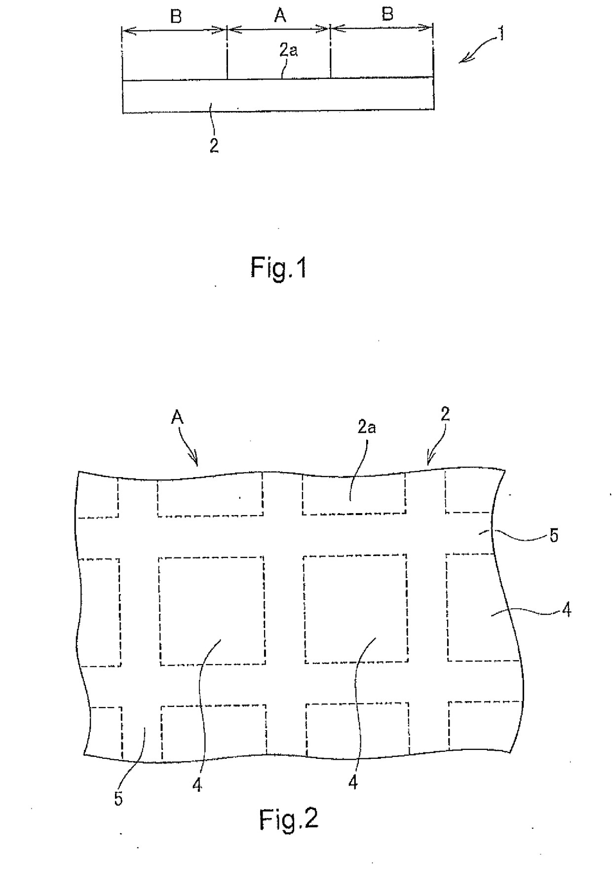
[0177]Next, a chromium thin film was formed on the surface of the base by a sputtering method. Then, an electron beam positive resist was applied onto the chromium thin film by a spin coating method. A desired resist pattern was formed on a hard mask material layer in the uneven structure area by performing electron beam drawing based on design coordinates on the application film and performing development. In the design coordinates, rectangular main pattern areas (1530 μm×1320 μm) were set so as to form a grid, and non-main pattern areas were set so as to form a lattice in gap portions of the individual main pattern areas (see FIG. 2). Square measurement areas (100 μm×100 μm) were set at 352 positions in the intersection portions of the non-main pattern areas. Further, in each measu...

example 2

[0188]

[0189]Four non-drawing areas each having a rectangular plan view shape (1 μm×8 μm) were set so as to be positioned at individual sides of a 12-μm square in each measurement area of the design coordinates of the electron beam drawing. In addition, along long sides of the four rectangular non-drawing areas, pixel areas in the line / space shape (line: 0.2 μm, space: 0.2 μm) that were disposed such that the longitudinal direction of each line was orthogonal to the long side, and had the length of each line of 1 μm were set. Further, a drawing area in the line / space shape (line: 0.2 μm, space: 0.2 μm) that was disposed such that the longitudinal direction of each line matched the Y direction (see FIG. 12) was set in the measurement area other than the pixel area and the non-drawing areas described above. The master mold was fabricated in the same manner as in Example 1 except that each measurement area was set in the above manner.

[0190]The master mold included, in each measurement a...

example 3

[0202]

[0203]As a flat plate-like base, a quartz glass substrate (152 mm×152 mm, thickness 6.35 mm) was prepared, and an uneven structure area of 25 mm×30 mm was set at the center of a surface of the base.

[0204]Next, a chromium thin film was formed on the surface of the base by the sputtering method. Then, an electron beam-sensitive positive resist was applied onto the chromium thin film by the spin coating method. A desired resist pattern was formed on a hard mask material layer in the uneven structure area by performing electron beam drawing based on design coordinates on the application film and performing development. In the design coordinates, rectangular main pattern areas (1530 μm×1320 μm) were set so as to form a grid, and non-main pattern areas were set so as to form a lattice in gap portions of the individual main pattern areas. Square measurement areas (100 μm×100 μm) were set at 352 positions in the intersection portions of the non-main pattern areas (see FIG. 17). Furthe...


PUM

PropertyMeasurementUnit
constant angleaaaaaaaaaa
length L2aaaaaaaaaa

Abstract

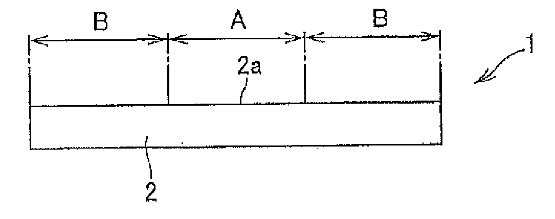
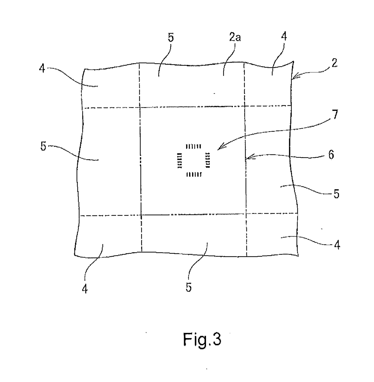
An imprint mold has a base 2, an uneven structure area A set on a surface 2a of the base 2, a measurement area 6 set in the uneven structure area A, and a measurement mark structure 7 positioned in the measurement area 6, the measurement mark structure 7 having a plurality of pattern sets 7a each having a line / space shape. With this, a deformation occurring in a resin layer at the time of release of the resin layer from the mold is prevented, and a measurement mark can be formed with high accuracy.

Description

TECHNICAL FIELD[0001]The present invention relates to an imprint mold having an uneven structure and an imprint method that uses the mold.BACKGROUND ART[0002]In recent years, as a fine pattern formation technique that replaces photolithography, a pattern formation technique that uses an imprint method attracts attention. The imprint method is the pattern formation technique in which one-to-one transfer of a fine structure is performed by using a mold member (mold) having a fine uneven structure and transferring the uneven structure to a molded resin. For example, in the imprint method in which a photo-curable resin is used as the molded resin, droplets of the photo-curable resin are supplied to the surface of a transfer substrate, a mold having a desired uneven structure and the transfer substrate are brought close to each other until the distance therebetween becomes a predetermined distance and the uneven structure is thereby filled with the photo-curable resin, light is emitted f...

Claims


Application Information

Patent Timeline
Patent Type & Authority Applications(United States)
IPC IPC(8): B05D3/12B05D3/06G03F7/00
CPCB05D3/12B05D3/067G03F7/0002B29C59/02H01L21/027G03F7/70775G03F9/7073
Inventor NAKATA, NAOKOYOSHIDA, KOUJIKAWAMATA, NAOSHINAGAI, TAKAHARUICHIMURA, KOJI
Owner DAI NIPPON PRINTING CO LTD
Learn More