Package structure and manufacturing method thereof
- Summary
- Abstract
- Description
- Claims
- Application Information
AI Technical Summary
Benefits of technology
Problems solved by technology
Method used
Image

Examples
first embodiment
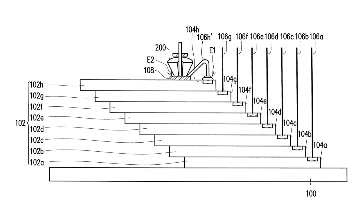
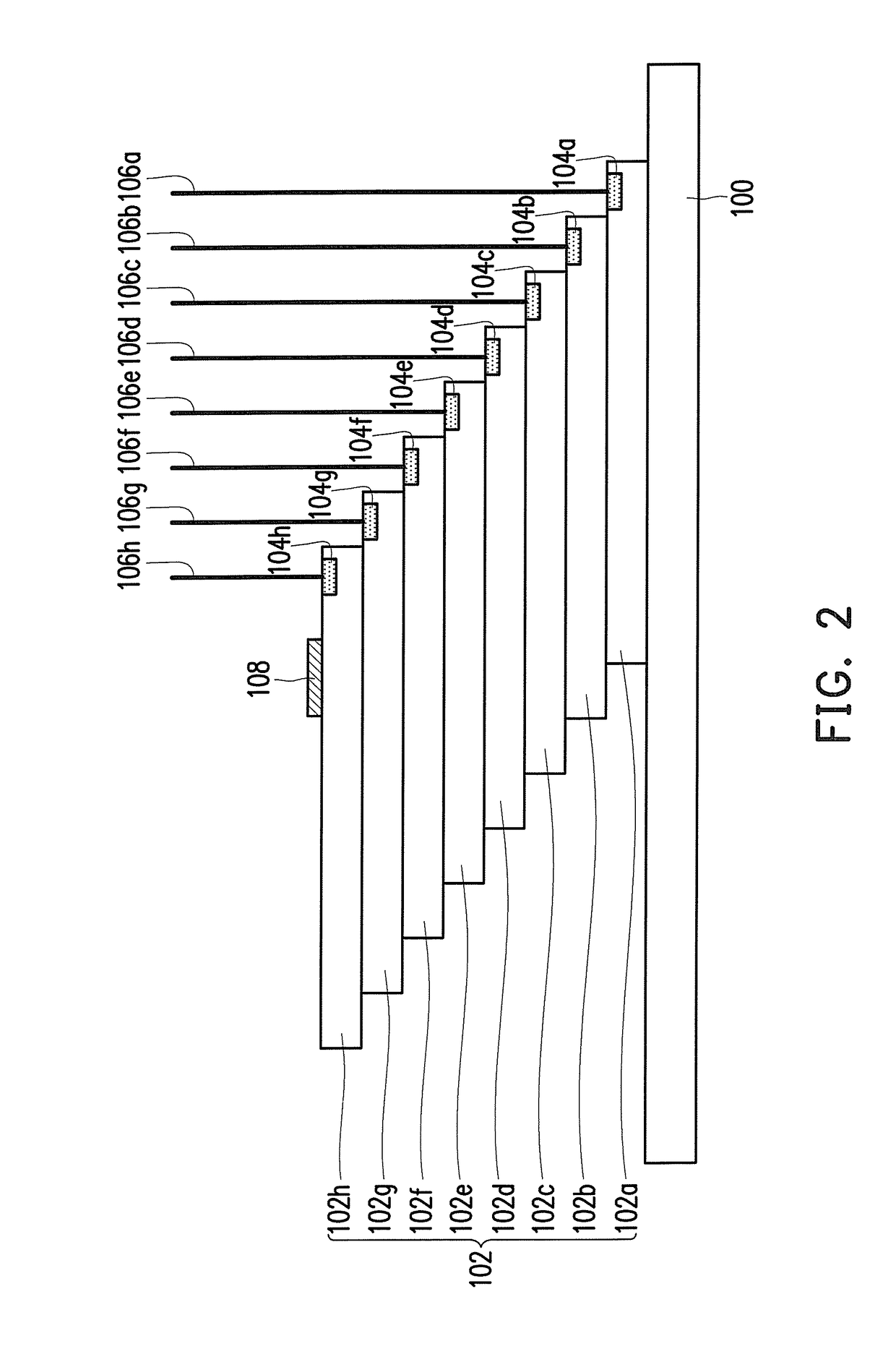
[0023]FIG. 2 is a schematic view illustrating a package structure according to the invention.
[0024]Referring to FIG. 2, the package structure of this embodiment includes a substrate 100, a multi-die stack structure 102, a plurality of first pads 104a to 104h, a plurality of vertical wires 106a to 106h, and a second pad 108. The multi-die stack structure 102 includes a plurality of dies 102a to 102h stacked alternately on the substrate 100. In this embodiment, the substrate 100 may be a printed circuit board, a silicon substrate, or a semiconductor substrate, for example.
[0025]The dies 102a to 102h include, from bottom to top, the first die 102a to the eighth die 102h. The first die 102a may be a bottom die, for example, and the eighth die 102h may be a top die, for example. In an embodiment, the multi-die stack structure 102 may be a step-like stack structure, for example. In an embodiment, the dies 102a to 102h may be dies having the same or different functions. However, the invent...
second embodiment
[0037]FIG. 4 is a schematic view illustrating a package structure according to the invention.
[0038]Referring to FIG. 4, the package structure of the second embodiment is similar to the package structure of the first embodiment, except for a main difference that the package structure of the second embodiment includes at least one third pad 110 disposed on the die 102d. The third pad 110 is disposed between a side of the die 102e and the vertical wire 106d of the die 102d. The third pad 110 may also serve as a dummy pad for wire cutting. Also, the third pad 110 may protect the die 102d therebelow, so as to be subjected to multiple wire bonding processes. Even though FIG. 4 only illustrates one third pad 110, the invention is not limited thereto. In other embodiments, one or more third pads 110 may be respectively disposed on any die between the bottom die and the top die. In an embodiment, a material of the third pad 110 is different from the material of the first pads 104a to 104h. I...
third embodiment
[0039]FIG. 5 is a schematic view illustrating a package structure according to the invention.
[0040]Referring to FIG. 5, the package structure of the third embodiment is similar to the package structure of the first embodiment, except for a main difference that the package structure of the third embodiment does not include the second pad 108 disposed on the top die 102h. More specifically, each of the dies 102a to 102h includes a first region R1, a second region R2, and a third region R3 of the third embodiment. The second region R2 is disposed between the first region R1 and the third region R3. An upper die may be disposed on the first region of a lower die, so as to form the step-like stack structure. For example, the die 102b is disposed on the first region R1 of the die 102a, so as to expose a surface of the die 102a in the second region R2 and the third region R3. The same arrangement applies to rest of the dies and may be construed through inference. Thus, details in this resp...
PUM
 Abstract
Description
Claims
Application Information
 - R&D
- Intellectual Property
- Life Sciences
- Materials
- Tech Scout
- Unparalleled Data Quality
- Higher Quality Content
- 60% Fewer Hallucinations
Browse by: Latest US Patents, China's latest patents, Technical Efficacy Thesaurus, Application Domain, Technology Topic, Popular Technical Reports.
© 2025 PatSnap. All rights reserved.Legal|Privacy policy|Modern Slavery Act Transparency Statement|Sitemap|About US| Contact US: help@patsnap.com