Resistive random access memory device

Inactive Publication Date: 2017-04-27
WINBOND ELECTRONICS CORP
View PDF10 Cites 7 Cited by
  • Summary
  • Abstract
  • Description
  • Claims
  • Application Information

AI Technical Summary

Problems solved by technology

However, the oxygen atoms may diffuse back to the resistive switching layer o

Method used


Image

  • Resistive random access memory device
  • Resistive random access memory device
  • Resistive random access memory device

Examples


Embodiment Construction

[0011]The following description is of the best-contemplated mode of carrying out the disclosure. This description is made for the purpose of illustrating the general principles of the disclosure and should not be taken in a limiting sense. The scope of the disclosure is best determined by reference to the appended claims.

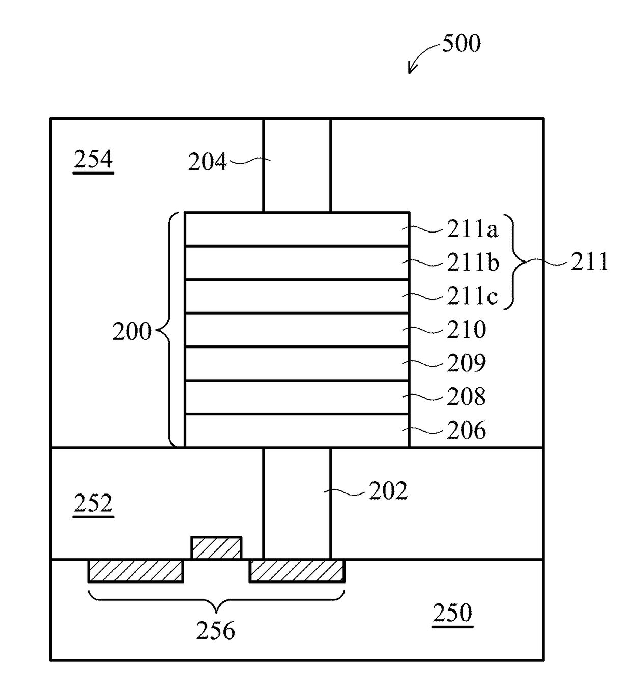
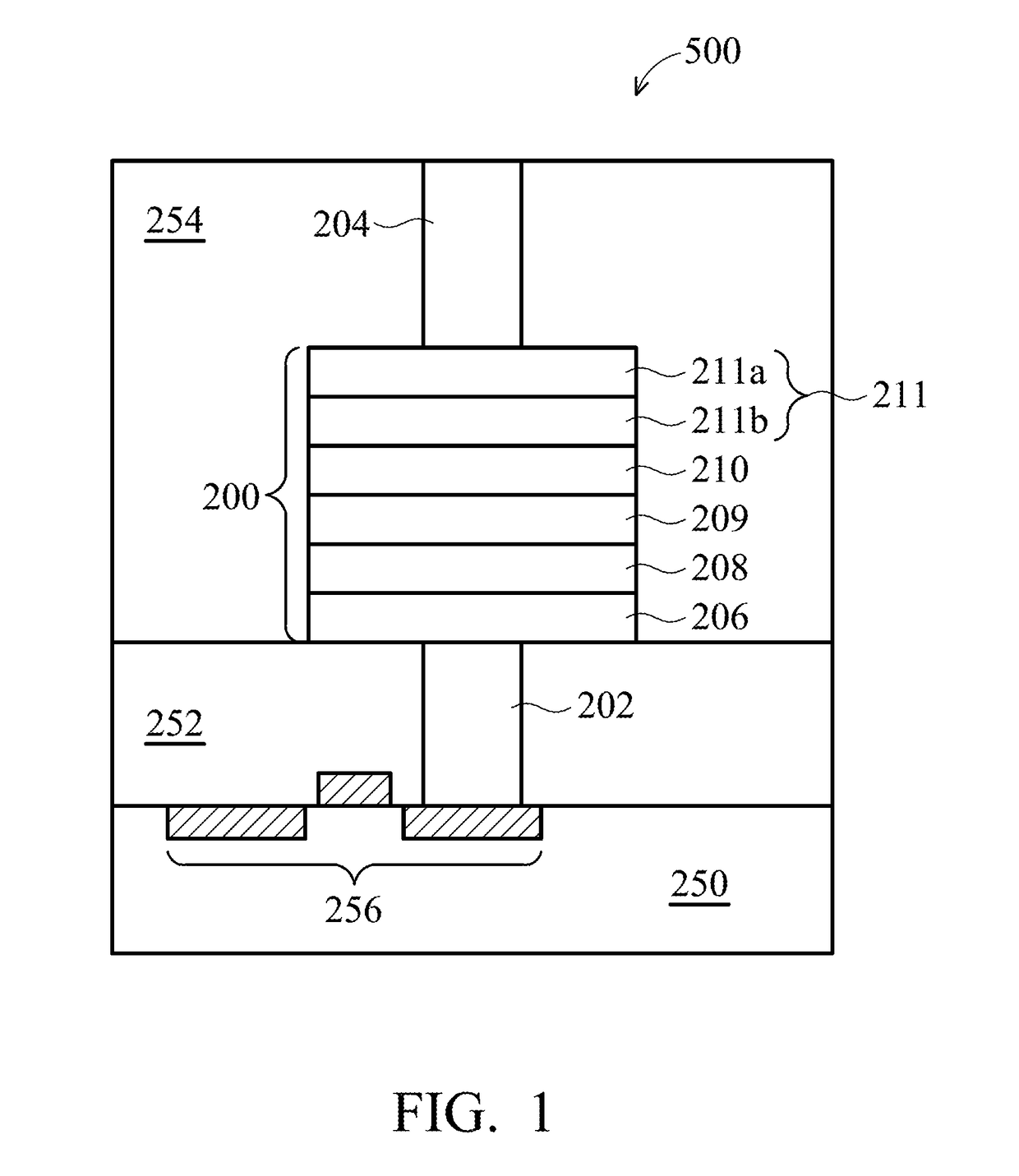
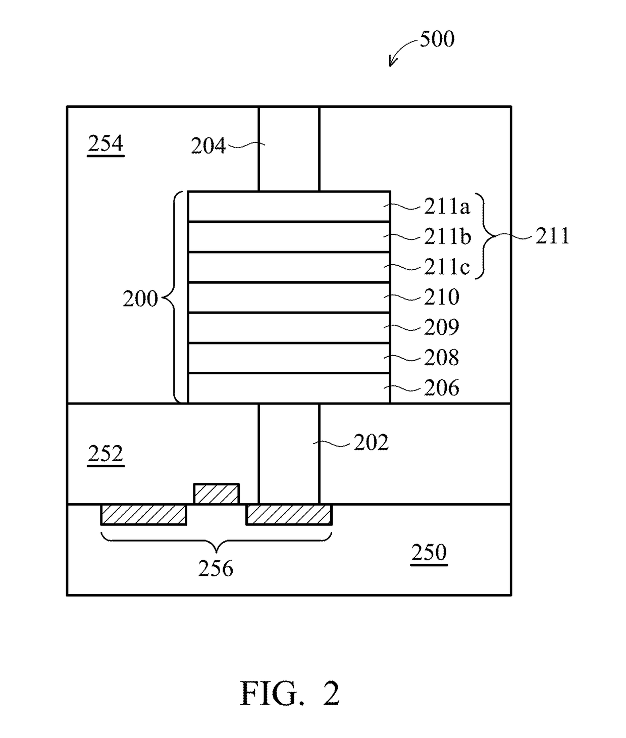
[0012]In one embodiment, a non-volatile memory such as a resistive random access memory (RRAM) device is provided. In a conventional RRAM device, the oxygen in the top electrode (migrating from a resistive switching layer by applying a voltage to the RRAM device) may diffuse back (down-toward) to the resistive switching layer, or escape out (upward) of the top electrode. The above oxygen diffusion and escape may cause the RRAM device to be ineffective. A novel RRAM stack structure is provide here to overcome the above oxygen diffusion / escape problem.

[0013]FIG. 1 shows a cross-sectional view of a RRAM device 500 in one embodiment. As shown in FIG. 1, the RRAM device ...


PUM


Abstract

A resistive random access memory device is provided, which includes a bottom electrode, a resistive switching layer disposed on the bottom electrode, an oxidizable layer disposed on the resistive switching layer, a first oxygen diffusion barrier layer disposed between the oxidizable layer and the resistive switching layer, and a second oxygen diffusion barrier layer disposed on the oxidizable layer.

Description

BACKGROUND[0001]Technical Field[0002]The disclosure relates to a resistive random access memory (RRAM) device, and in particular it relates to a stack structure of the RRAM device.[0003]Description of the Related Art[0004]The resistive random access memory (RRAM) device has become a major stream of the newly developed non-volatile memory due to the following advantages: low power consumption, low operation voltage, short write and erase times, long endurance, long data retention time, non-destructive read operation, multi-state memory, simple manufacture, and scalable properties. The basic structure of the RRAM device includes a metal-insulator-metal (MIM) stack of a bottom electrode, a resistive switching layer, and a top electrode. The resistive switching (RS) property is an important property of the RRAM device. For example, when a writing voltage (turn-on voltage) is applied to the RRAM device, the oxygen atoms in the resistive switching layer may migrate to the top electrode to...

Claims


Application Information

Patent Timeline
IPC IPC(8): H01L45/00
CPCH01L45/08H01L45/1233H01L45/146H01L45/1246H01L45/1253H10N70/24H10N70/20H10N70/801H10N70/841H10N70/826H10N70/8833H10N70/828
Inventor CHEN, FREDERICKLIAO, SHAO-CHINGWANG, PING-KUN
Owner WINBOND ELECTRONICS CORP
Why Eureka
Try Eureka