Ltps array substrate and method for producing the same

Active Publication Date: 2017-05-18
TCL CHINA STAR OPTOELECTRONICS TECH CO LTD +1
View PDF4 Cites 1 Cited by
  • Summary
  • Abstract
  • Description
  • Claims
  • Application Information

AI Technical Summary

Benefits of technology

[0020]The fact about the LTPS array substrate and the method for producing the LTPS array substrate proposed by the present invention is that one side of a substrate on the opposite side of a gate is exposed for forming a polycrystalline silicon layer. In other words, an opaque gate

Problems solved by technology

However, the LTPS technology is sophisticated.
Also, it needs many processes to produc

Method used


Image

  • Ltps array substrate and method for producing the same
  • Ltps array substrate and method for producing the same
  • Ltps array substrate and method for producing the same

Examples


Embodiment Construction

[0028]The drawings illustrate embodiments of the invention and, together with the description, serve to explain the principles of the invention.

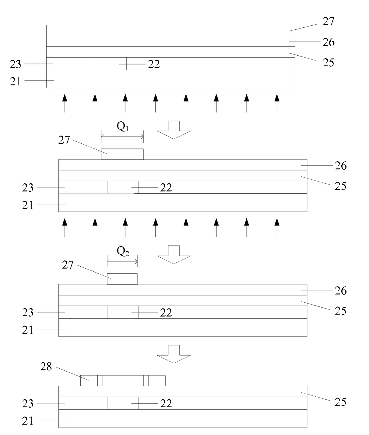
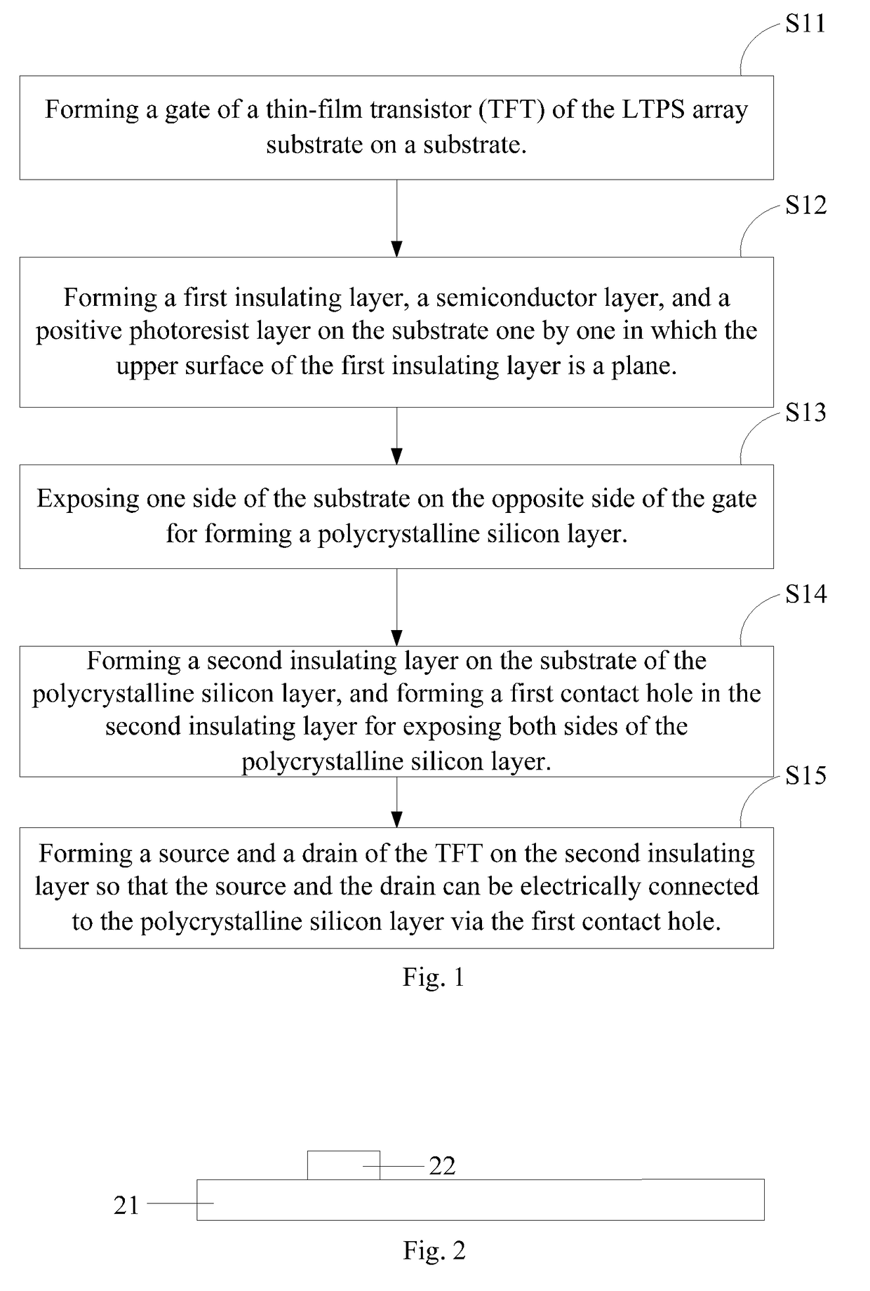
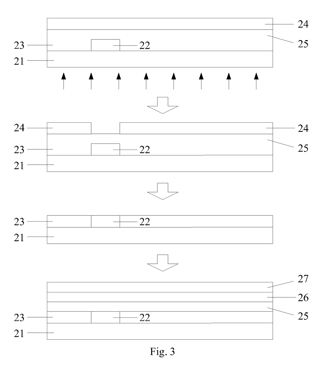
[0029]FIG. 1 is a flow chart of a method for producing an LTPS array substrate according to one embodiment of the present invention. The method comprises following steps of:

[0030]Step 11: Forming a gate of a thin-film transistor (TFT) of the LTPS array substrate on a substrate.

[0031]Please refer to FIG. 2. The substrate 21 is used for forming the LTPS array substrate of an LCD panel. The substrate 21 can be a glass substrate, a plastic substrate, or a flexiblesubstrate.

[0032]A first metallic layer is formed on the substrate 21 and the first metallic layer is exposed through a first mask in this embodiment. The exposed first metallic layer is patterned after being developed and etched. Then, a gate 22 is formed. The first metallic layer is etched with etching liquid comprising phosphoric acid, nitric acid, acetic acid, and deionized water. Ce...


PUM


Abstract

An LTPS array substrate and a method for producing the same are proposed. The method includes: forming a gate of a thin-film transistor (TFT) of the LTPS array substrate on a substrate; forming a first insulating layer, a semiconductor layer, and a positive photoresist layer on the substrate one by one; exposing one side of the substrate on the opposite side of the gate for forming a polycrystalline silicon layer; forming a second insulating layer on the substrate of the polycrystalline silicon layer; forming a source and a drain of the TFT on the second insulating layer so that the source and the drain is electrically connected to the polycrystalline silicon layer via a contact hole. The use of masks in types and in numbers in the LTPS technology will be reduced. So, both of the processes and the production costs are reduced.

Description

BACKGROUND OF THE INVENTION[0001]1. Field of the Invention[0002]The present invention relates to the field of display technology, and more particularly, to a low temperature poly-silicon (LTPS) array substrate and a method for producing the LTPS array substrate.[0003]2. Description of the Prior Art[0004]Higher electron mobility is demonstrated in a liquid crystal display (LCD) adopting LTPS. The square of a thin film transistor (TFT) is actually smaller in this kind of LCD in which the aperture rate of a pixel is higher, and the brightness is larger. Anyway, power consumption and production costs are less using an LCD with LTPS. Owing to these features, the research on the LCD with LTPS is popular in LCD technology. However, the LTPS technology is sophisticated. It requires a lot of masks in various types to fabricate an array substrate (array substrate). Also, it needs many processes to produce an array substrate. Therefore, production costs are always high, which is a problem. To ...

Claims


Application Information

Patent Timeline
IPC IPC(8): H01L27/12H01L29/786H01L29/66
CPCH01L27/1288H01L29/78618H01L29/78678H01L29/66765H01L27/124H01L27/1248
Inventor WANG, CONGDU, PENG
Owner TCL CHINA STAR OPTOELECTRONICS TECH CO LTD
Why Eureka
Try Eureka