Liquid crystal display panel and liquid crystal display device

a liquid crystal display panel and display panel technology, applied in the field of displays, can solve the problems of high manufacturing cost, inability to reduce the size of printed circuit boards, and difficulty in the manufacture of printed circuit boards to meet the small size of panels, and achieve the effect of reducing the size and the cost of liquid crystal display panels

Inactive Publication Date: 2017-05-25
SHENZHEN CHINA STAR OPTOELECTRONICS TECH CO LTD
View PDF5 Cites 2 Cited by
  • Summary
  • Abstract
  • Description
  • Claims
  • Application Information

AI Technical Summary

Benefits of technology

[0006]A primary object of the present invention is to provide a liquid crystal display panel and a li

Problems solved by technology

There are many chips disposed on the printed circuit board in the first driving mode and the second driving mode, thus the size of the printed circuit board cannot be red

Method used


Image

  • Liquid crystal display panel and liquid crystal display device
  • Liquid crystal display panel and liquid crystal display device
  • Liquid crystal display panel and liquid crystal display device

Examples


Embodiment Construction

[0031]The structure and the technical means adopted by the present invention to achieve the above and other objects can be best understood by referring to the following detailed description of the preferred embodiments and the accompanying drawings. Furthermore, directional terms described by the present invention, such as upper, lower, front, back, left, right, inner, outer, side, longitudinal / vertical, transverse / horizontal, etc. are only directions by referring to the accompanying drawings, and thus the used directional terms are used to describe and understand the present invention, but the present invention is not limited thereto.

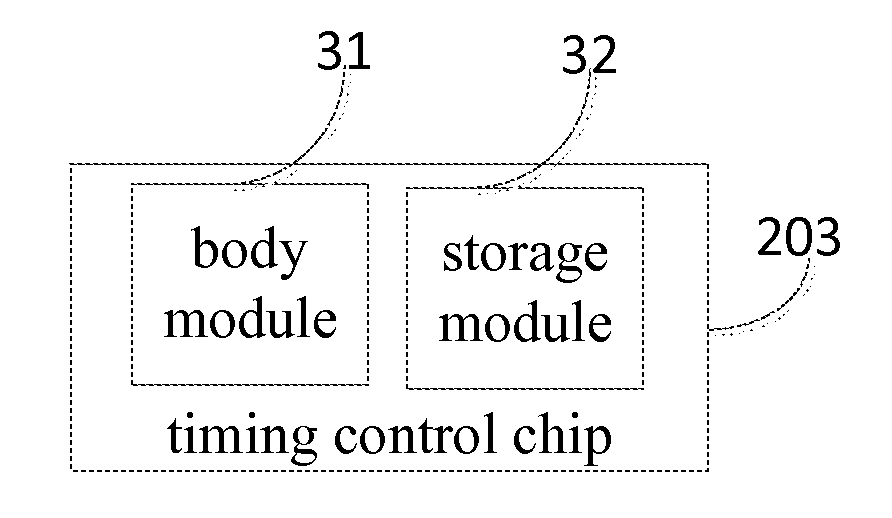
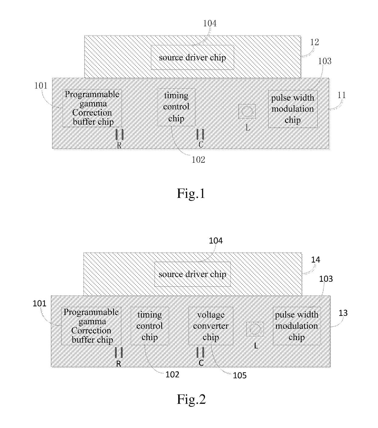
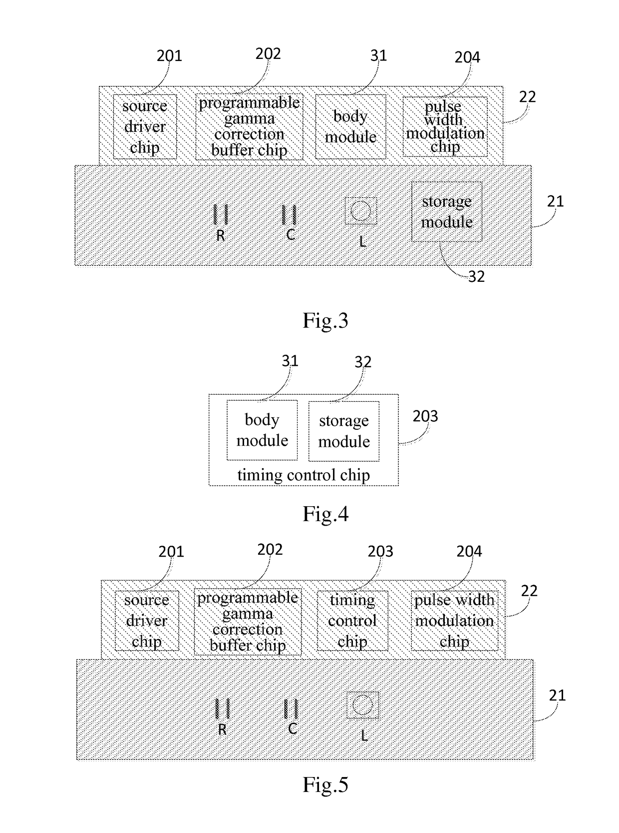
[0032]Refer to FIG. 3, which is a schematic view of a first type driving portion of the first type liquid crystal display panel according to a preferred embodiment of the present invention.

[0033]The first type liquid crystal display panel of the present invention with a common driving mode having a body portion and a driving portion. The body portion i...


PUM


Abstract

A liquid crystal display panel and a liquid crystal display device are provided. The panel has a driving portion including a plurality of chips and a plurality of electronic components. The chips comprise a source driver chip, a pulse width modulation chip, a programmable gamma correction buffer chip, and a timing control chip. The electronic components are disposed on the printed circuit board. The source driver chip, the pulse width modulation chip, and the programmable gamma correction buffer chip are disposed on the flexible connector.

Description

FIELD OF THE INVENTION[0001]The present invention relates to a technical field of displays, and in particular to a liquid crystal display panel and a liquid crystal display device.BACKGROUND OF THE INVENTION[0002]A liquid crystal display panel with a common driving mode (first type driving mode) has a body portion and a driving portion. The body portion includes a plurality of data lines, a plurality of scan lines, and a plurality of pixel units defined by the data lines and the scan lines. Refer to FIG. 1, the driving portion has a printed circuit board 11 and a flexible connector 12. A programmable gamma correction buffer chip 101, a timing control chip 102, a pulse width modulation chip 103, and electronic components (such as resistors, capacitors, and inductors) are disposed on the printed circuit board 11. A source driver chip 104 is disposed on the flexible connector 12.[0003]As compared with the liquid crystal display panel with the common driving mode, a liquid crystal displ...

Claims


Application Information

Patent Timeline
IPC IPC(8): G09G3/36
CPCG09G3/3648G09G3/3677G09G2320/064G09G2310/08G09G2300/0426G09G2320/0276G09G3/3611G02F1/13452
Inventor CHEN, YINHUNGLI, YUNTAO
Owner SHENZHEN CHINA STAR OPTOELECTRONICS TECH CO LTD
Why Eureka
Try Eureka