Liquid crystal display panel, display device, and driving method

Inactive Publication Date: 2017-05-25
WUHAN CHINA STAR OPTOELECTRONICS TECH CO LTD
View PDF2 Cites 7 Cited by
  • Summary
  • Abstract
  • Description
  • Claims
  • Application Information

AI Technical Summary

Benefits of technology

[0017]According to the embodiments of the present disclosure, the scanning signal can be provided to the first scanning line and the second scanning line simultaneously during one time-sequence, and the data can also be transmitted to the first data line and the second data line simultaneously during said time-sequence, so that the pixel electr

Problems solved by technology

As a result, the charge time of the pixel electrode is insuffici

Method used


Image

  • Liquid crystal display panel, display device, and driving method
  • Liquid crystal display panel, display device, and driving method
  • Liquid crystal display panel, display device, and driving method

Examples


Example

Embodiment 1

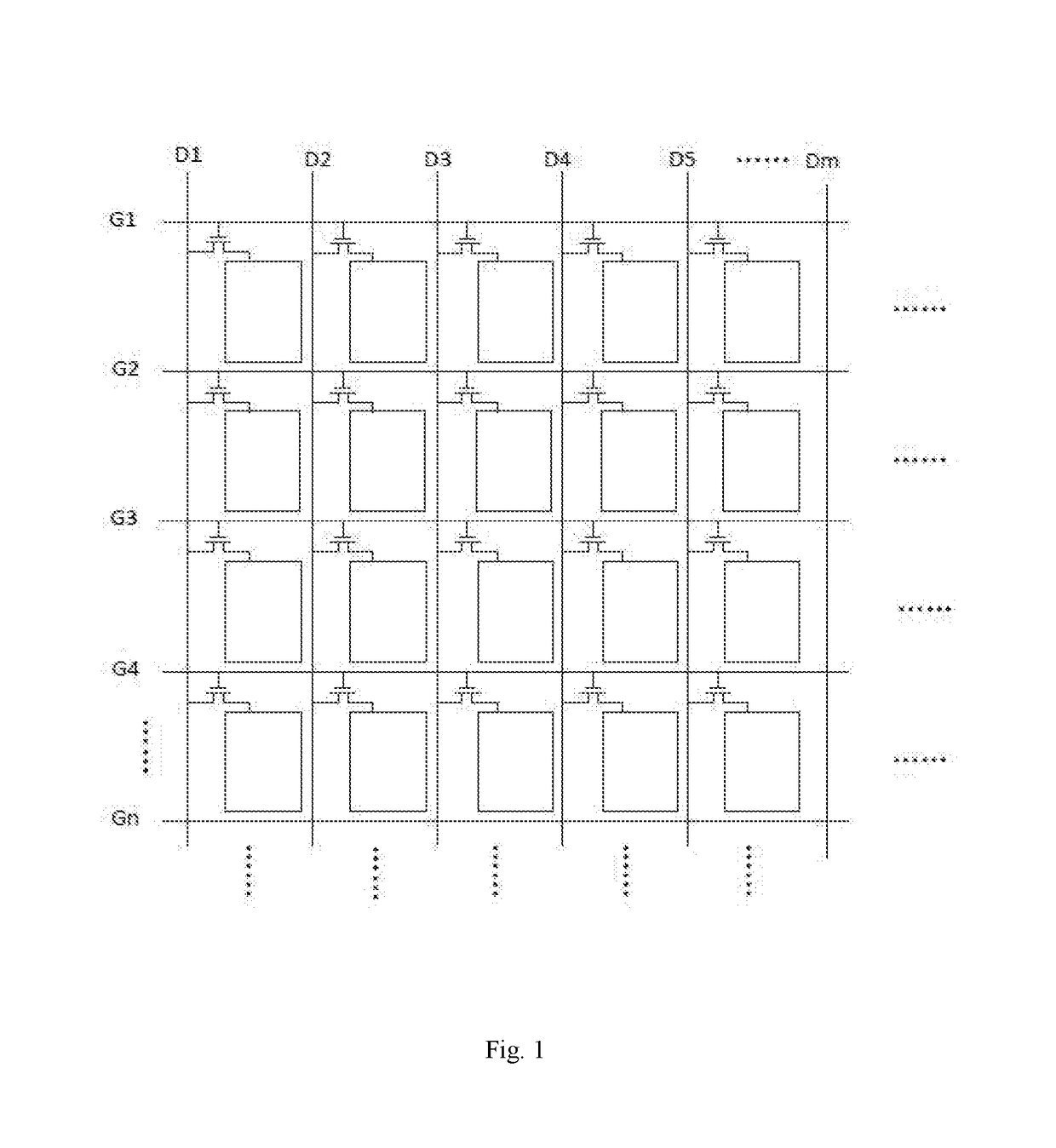
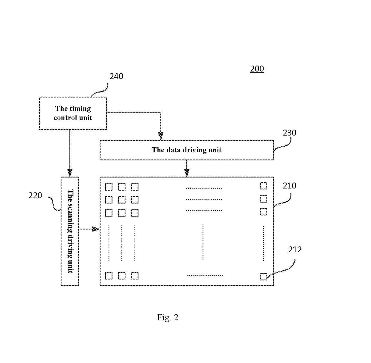
[0032]FIG. 2 schematically shows a structure of a liquid crystal display device 200 according to the present embodiment. As shown in FIG. 2, the liquid crystal display device 200 comprises a display panel 210, a scanning driving unit 220, a data driving unit 230, and a timing control unit 240. The display panel 210 comprises a plurality of pixel units 212 that are arranged in an array.

[0033]The scanning driving unit 220 and the data driving unit 230 are electrically connected with the display panel 210 respectively. The timing control unit 240 is electrically connected with the scanning driving unit 220 and the data driving unit 230, so that the display panel 210 can be scanned by the scanning driving unit 220 and be driven by the data driving unit 230 under the control of the timing control unit 240 and the image can be displayed.

[0034]FIG. 3 schematically shows a structure of a display panel 210 according to the present embodiment. According to the present embodiment, ...

Example

Embodiment 2

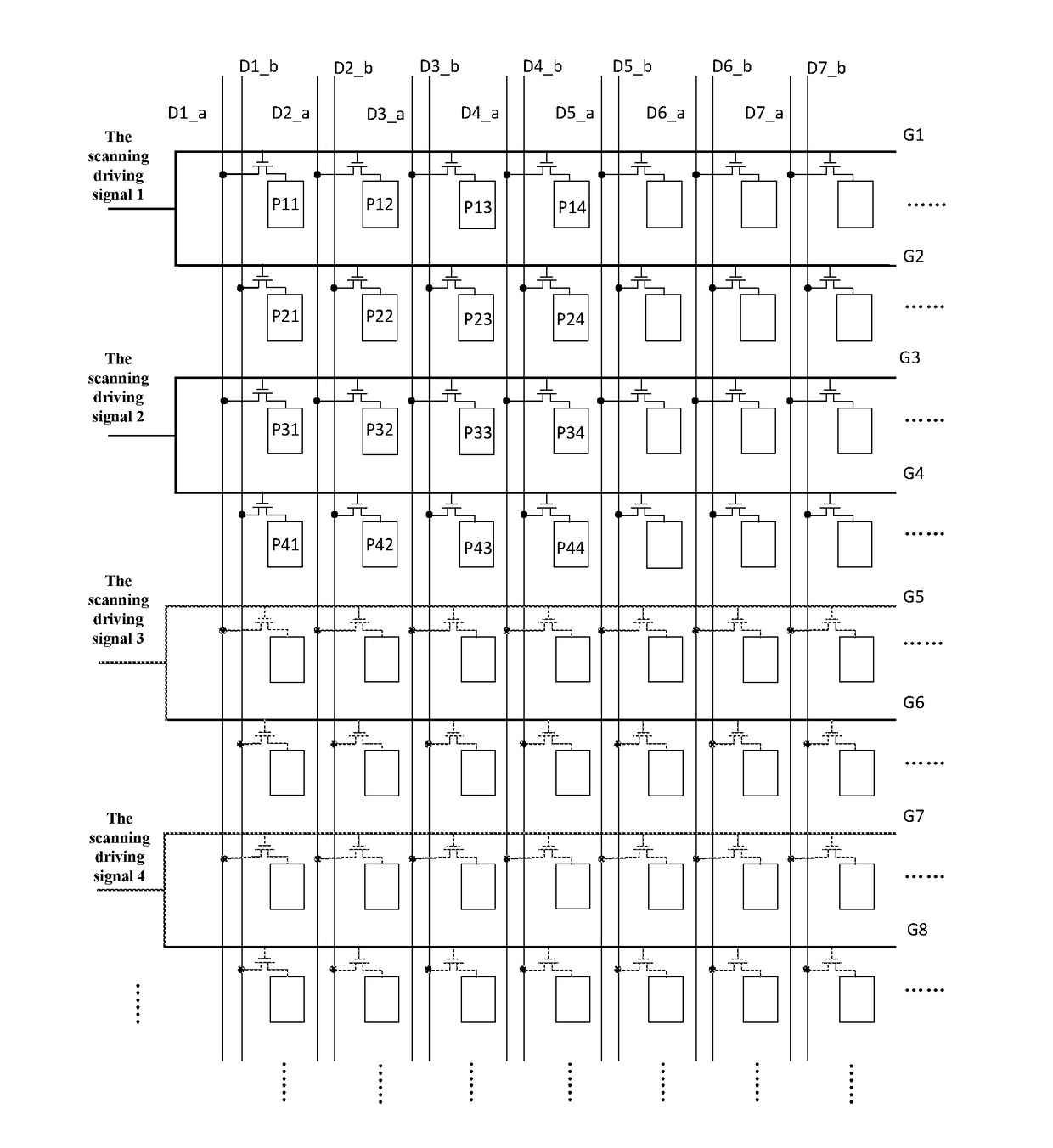
[0044]FIG. 6 schematically shows a structure of a liquid crystal display panel according to the present embodiment. The data lines are arranged in the same manner as embodiment 1, and the details of which are no longer repeated here. However, the scanning lines are arranged in a manner different from that of embodiment 1. As shown in FIG. 6, G1, G2, G5, and G6 are the first scanning lines, and G3, G4, G7, and G8 are the second scanning lines. The first scanning line G1 and the second scanning line G3 are separated by two rows of pixel units, and the first scanning line G2 and the second scanning line G4 are also separated by two rows of pixel units. The first scanning line G1 and the first scanning line G2 are arranged adjacent to each other, and the second scanning line G3 and the second scanning line G4 are arranged adjacent to each other.

[0045]In order to facilitate the illustration, according to the present embodiment, two consecutive first pixel units in each column...

Example

Embodiment 3

[0051]The present embodiment provides a technical solution that the first scanning line and the second scanning line are separated by k rows of pixel units. FIG. 8 schematically shows a structure of a liquid crystal display panel according to the present embodiment. G1, G2, . . . , and G(k) are the first scanning lines, and G(k+1), G(k+2), . . . , and G(n) are the second scanning lines. In order to facilitate the understanding, according to the present embodiment, n is preferably selected to be an even number, and k=n / 2. As shown in FIG. 8, the first scanning line G1 and the second scanning line G(k+1) are separated by k rows of pixel units, k first scanning lines are arranged adjacent to each other, and k second scanning lines are arranged adjacent to each other.

[0052]Taking the pixel units in the first column as an example, the pixel units P11, P21, . . . , and Pk1 constitute the first pixel unit group, and the pixel units P(k+1)1, . . . , and Pn1 constitute the second...


PUM


Abstract

A liquid crystal display panel, a display device, and a driving method thereof are disclosed. The liquid crystal display panel comprises a plurality of data line pairs, a plurality of scanning lines, and a pixel unit array, wherein the first scanning line and the second scanning line turn on TFT switches of two rows of pixel units simultaneously according to a scanning driving signal, and the first data line and the second data line charge the pixel electrodes of two rows of pixel units through the TFT switches according to a data driving signal.

Description

CROSS REFERENCE TO RELATED APPLICATION[0001]The present application claims benefit of Chinese patent application CN 201510274900.X, entitled “Liquid Crystal Display Panel, Display Device, and Driving Method” and filed on May 26, 2015, the entirety of which is incorporated herein by reference.FIELD OF THE INVENTION[0002]The present disclosure relates to the technical field of liquid crystal display, and particularly to a liquid crystal display panel, a display device, and a driving method thereofBACKGROUND OF THE INVENTION[0003]In a liquid crystal display device in the prior art, images are generally displayed in a line-by-line scanning driving method. As shown in FIG. 1, the liquid crystal display panel comprises a plurality of pixel units that are defined by a plurality of scanning lines (G1 to Gn) and a plurality of data lines (D1 to Dm) crossing over with one another, and each pixel unit comprises a pixel electrode. When the line-by-line scanning is performed, a scanning signal i...

Claims


Application Information

Patent Timeline
IPC IPC(8): G09G3/36G02F1/1362G02F1/1368
CPCG09G3/3677G02F1/1368G02F1/136286G09G2310/0251G02F2201/123G09G2300/0809G09G3/3688G02F1/13306G09G2310/021G09G3/3648
Inventor XING, ZHENZHOUZUO, QINGCHENGHUANG, CHUN HUNG
Owner WUHAN CHINA STAR OPTOELECTRONICS TECH CO LTD
Why Eureka
Try Eureka