Ultrasound sensor and method of manufacturing thereof

a technology of ultrasonic sensors and manufacturing methods, applied in the field of ultrasonic sensors, can solve the problems of difficult use, different piezoelectric materials to be arranged, etc., and achieve the effect of improving transmission performance and reception performan

Active Publication Date: 2017-06-08
SEIKO EPSON CORP
View PDF2 Cites 4 Cited by
  • Summary
  • Abstract
  • Description
  • Claims
  • Application Information

AI Technical Summary

Benefits of technology

[0014]In the aspect, the ultrasound elements which are optimized to the dedicated transmission type and the dedicated reception type can be manufactured and transmission performance and reception performance can be improved, respectively, only by varying a dimension of the second electrode (for example, a width of the second electrode) with areas of the dedicated transmission ultrasound element and the dedicated reception ultrasound element when forming the second electrode in a film-manufacturing process and when patterning the second electrode.

Problems solved by technology

That is, in a case where a dedicated transmission type element and a dedicated reception type element are provided, the elements having different piezoelectric materials have to be arranged, which is very difficult.
In a case of unifying the piezoelectric materials, even though the transmission sensitivity and the reception sensitivity are able to be adjusted by varying, for example, a size of an opening portion, it is practically and actually difficult to use since a resonance frequency will be varied according to the varied size of the opening.

Method used


Image

  • Ultrasound sensor and method of manufacturing thereof
  • Ultrasound sensor and method of manufacturing thereof
  • Ultrasound sensor and method of manufacturing thereof

Examples


embodiment 2

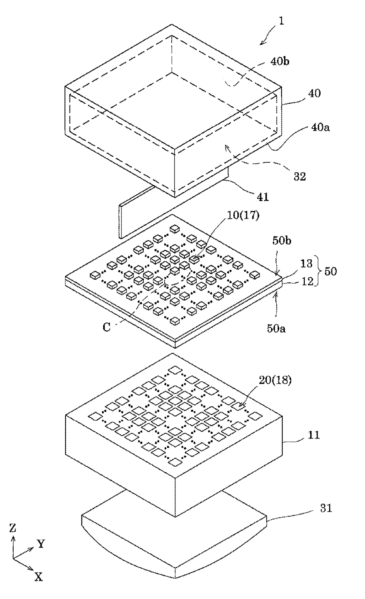
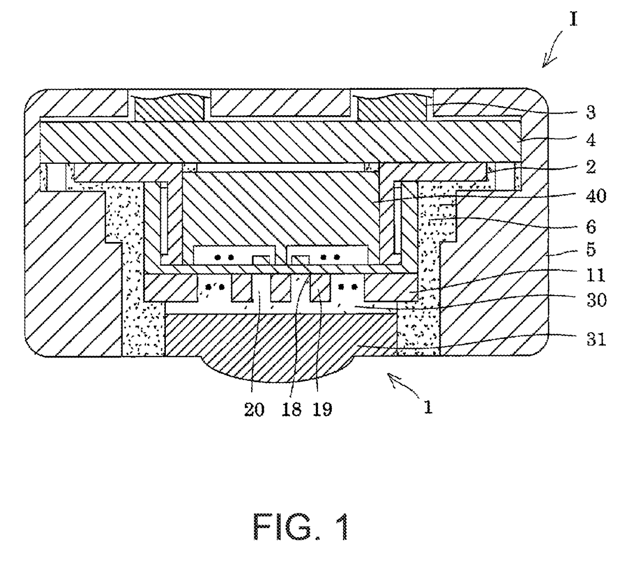
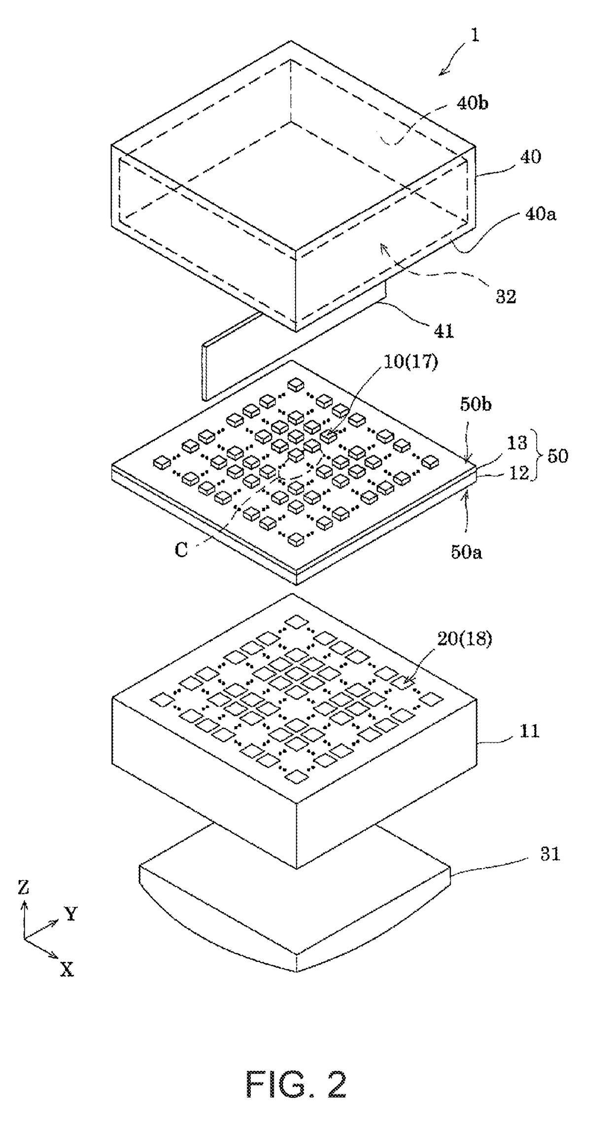
[0075]An ultrasound sensor 1A of Embodiment 2 will be described with reference to one example of the manufacturing method. Each of FIGS. 14 to 19 illustrates each process and includes a plan view and cross-sectional views taken along lines b-b′ and c-c′. In Embodiment 1 stated above, the second electrode 16 is a common electrode, but in Embodiment 2, the first electrode 14 is a common electrode.

[0076]First, as illustrated in FIGS. 14A, 14B and 14C, after forming an elastic film 12 formed of silicon oxide by thermal oxidation or the like of a substrate 11, a zirconium film is formed thereupon, and thermally oxidized at 500 to 1200° C., and an insulator film 13 formed of zirconium oxide is formed. The first electrode 14 is formed on the insulator film 13 by a sputtering method, a deposition method or the like, and patterning carried out so that the first electrode 14 takes a predetermined shape.

[0077]Next, as illustrated in FIGS. 15A, 15B and 15C, the piezoelectric layer 15 is layered...

embodiment 3

[0082]FIGS. 20A, 20B and 20C show an ultrasound sensor 1B of Embodiment 3. In the present embodiment, when patterning the secondary second electrode 16b, the second electrode 16 and a discontinuous electrode 22 which is electrically discontinued from the second electrode 16 are separated by a groove 21 instead of removing unnecessary portion of the second electrode 16. By varying a forming position of the groove 21, the wider second electrode 16A is provided in a center row in the vertical direction, the narrower second electrodes 16B are provided on both sides in the vertical direction, the dedicated transmission piezoelectric element 17A is provided in a center row and the dedicated reception piezoelectric elements 17B are provided on both sides in the vertical direction.

[0083]This process also enables that the dedicated transmission piezoelectric element 17A and the dedicated reception piezoelectric element 17B can be manufactured and transmission performance and reception perfor...

embodiment 4

[0084]FIGS. 21A and 21B show an ultrasound sensor 1C of Embodiment 4. In the present embodiment, the width of the first electrodes 14 is varied so as to serve as the dedicated transmission element and the dedicated reception element instead of varying the width of the second electrode 16. In the present embodiment, when patterning the first electrode 14, i.e. the common electrode, a center row in the vertical direction is subjected to patterning so as to be a wider first electrode 14A, and rows on both sides in the vertical direction are subjected to patterning so as to be a narrower first electrodes 14B. After that, the same processes as those of the embodiments stated above are employed. The dedicated transmission piezoelectric element 17A having the wider first electrode 14A is provided in the center row in the vertical direction, and the dedicated reception piezoelectric elements 17B having the narrower first electrodes 14B are provided in the rows on both sides in the vertical ...


PUM


Abstract

An ultrasound sensor includes: a diaphragm; a plurality of first electrodes; a plurality of second electrodes; and a plurality of piezoelectric layers which is provided between the first electrode and the second electrode, in which, in a Z-direction, a portion in which the first electrode, the piezoelectric layer and the second electrode are overlapped is referred to as an active portion, and a range to the extent that the diaphragm is oscillatable by driving the active portion is referred to as a movable portion, when a unit including one movable portion and the active portion which is provided within the one movable portion is referred to as one ultrasound element in plan view, two or more types of ultrasound elements in which a dimension of the active portion with respect to a dimension of the movable portion is different from each other in plan view are provided.

Description

CROSS-REFERENCE TO RELATED APPLICATIONS[0001]This application is a U.S. National Phase Application under 35 U.S.C. 371 of International Application No. PCT / JP2015 / 069810, filed on Jul. 9, 2015 and published in Japanese as WO 2016 / 006671 on Jan. 14, 2016. This application claims priority to Japanese Patent Application No. 2014-141778, filed on Jul. 9, 2014. The entire disclosures of the above applications are incorporated herein by reference.TECHNICAL FIELD[0002]The present invention relates to an ultrasound sensor and a method of manufacturing thereof.BACKGROUND ART[0003]Ultrasound sensors in which a semiconductor substrate having an opening portion, two layers of electrodes on an insulating film layer formed on the surface of the semiconductor substrate while blocking the opening portion and a PZT ceramic thin film layer interposed between the two layers of electrodes are arranged in an array form are known in the related art (for example, refer to JP-A-2010-164331).[0004]In such a...

Claims


Application Information

Patent Timeline
Patent Type & Authority Applications(United States)
IPC IPC(8): B06B1/06H01L41/29H01L41/31A61B8/00
CPCB06B1/0622H01L41/31H01L41/29A61B8/4427A61B8/4444A61B8/4488B06B1/0629G01S15/8925H10N30/06H10N30/07
Inventor KOJIMA, CHIKARA
Owner SEIKO EPSON CORP
Why Eureka
Try Eureka