Thin film transistor, method for manufacturing the same, and array substrate

a technology of thin film transistors and array substrates, which is applied in the direction of transistors, semiconductor devices, electrical equipment, etc., can solve the problems of reducing affecting the operation characteristics of tft devices, and affecting the quality of products, so as to reduce the mobility of carriers and effectively suppress leakage current, the effect of high resistan

Active Publication Date: 2017-06-08
BOE TECH GRP CO LTD
View PDF5 Cites 0 Cited by
  • Summary
  • Abstract
  • Description
  • Claims
  • Application Information

AI Technical Summary

Benefits of technology

[0028]As can be seen from the technical solutions above, the embodiments of present disclosure provide a thin film transistor, a method for manufacturing the same, and an array substrate, wherein the thin film transistor is provided with

Problems solved by technology

However, due to the high mobility of this material, leakage current of the TFT device is large, which has an adverse impact on operation characteris

Method used


Image

  • Thin film transistor, method for manufacturing the same, and array substrate
  • Thin film transistor, method for manufacturing the same, and array substrate
  • Thin film transistor, method for manufacturing the same, and array substrate

Examples


Embodiment Construction

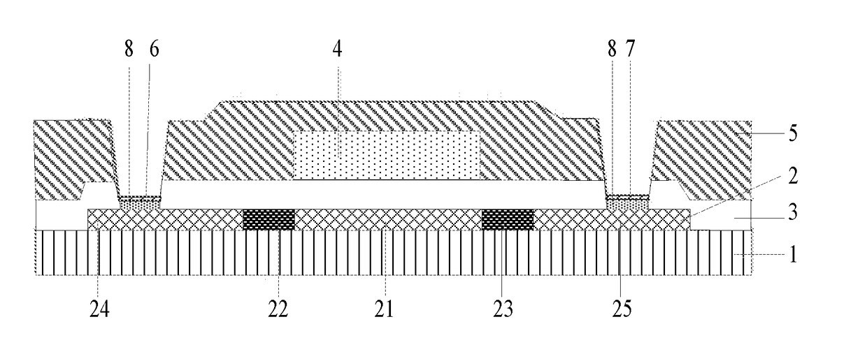
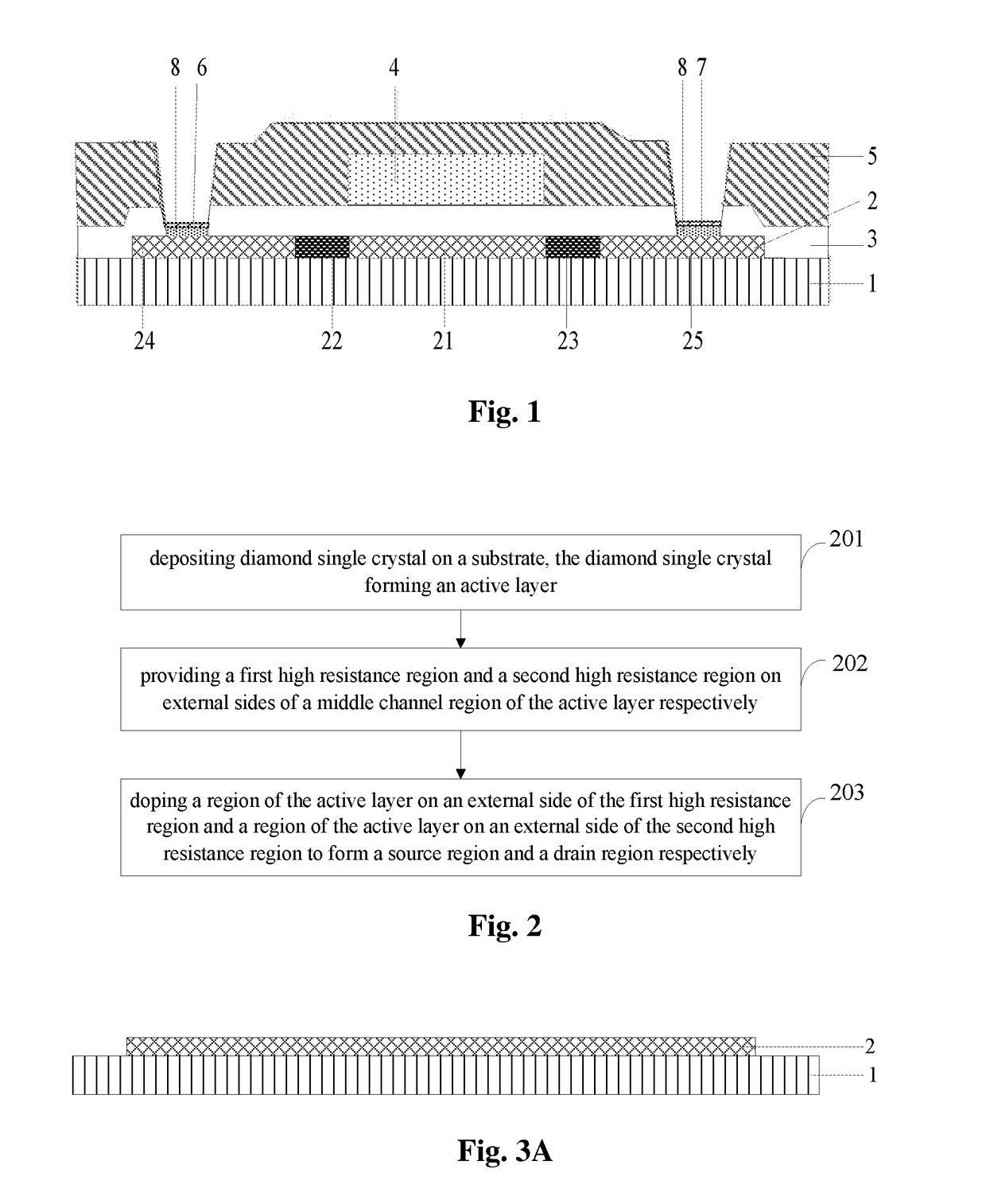
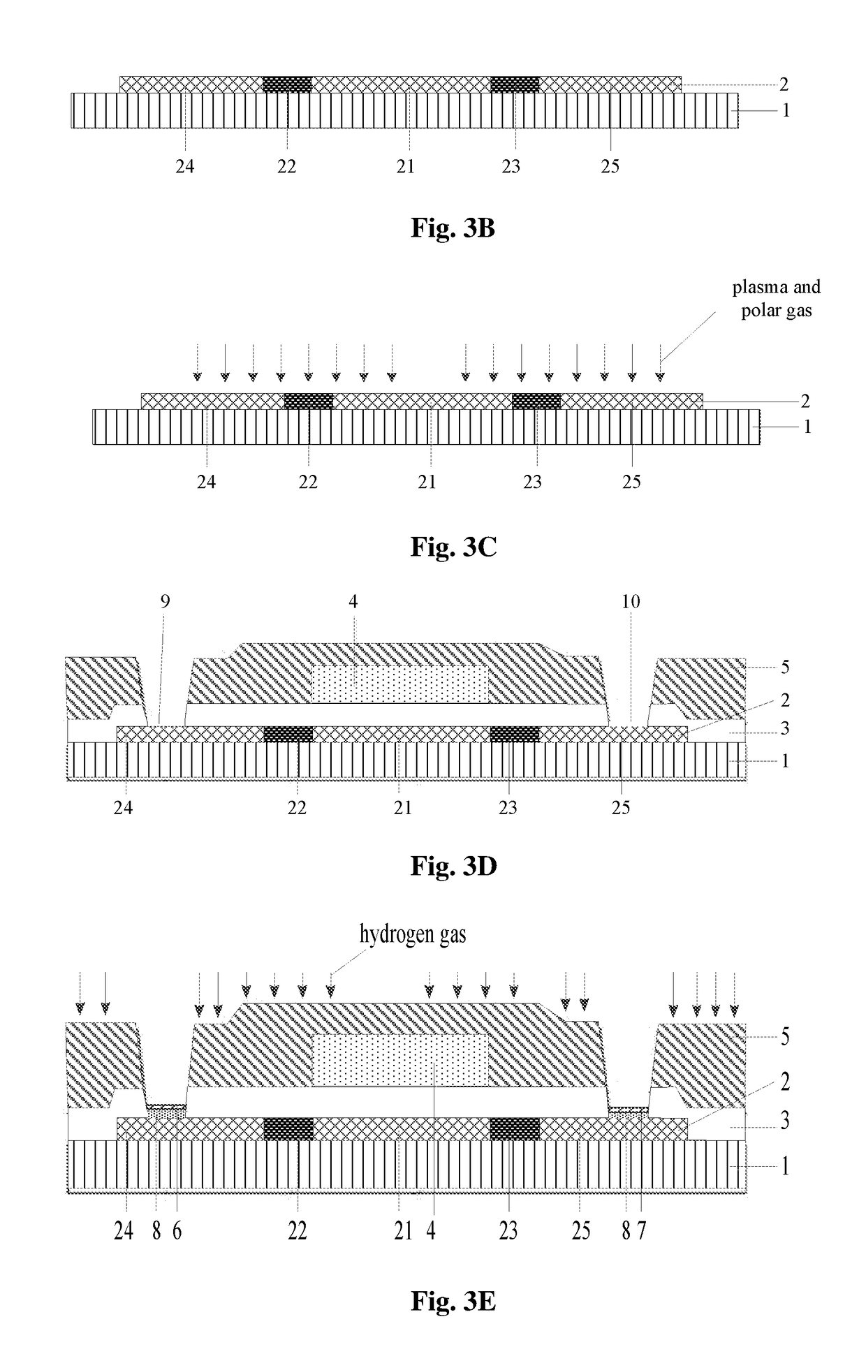
[0033]The technical solutions of the embodiments of the present invention will be described clearly and thoroughly hereinafter in conjunction with the drawings in respective embodiments in order to make the objects, technical solutions and advantages of the embodiments of the disclosure more clear. Obviously, the embodiments described are only some rather than all of the embodiments of the disclosure. All other embodiments obtained by one ordinary person skilled in the art based on the described embodiments in the disclosure without creative work are within the scope of the present disclosure.

[0034]In the description of the present disclosure, it should be noted that the oriental or positional relationship indicated by the terms “upper”, “lower”, “top” , “bottom” or the like is the oriental or positional relationship shown in the drawings, and such terms are used only for the purpose of description and simplifying the description rather than indicating or suggesting that the device ...


PUM


Abstract

The embodiments of present disclosure provide a thin film transistor, a method for manufacturing the same, and an array substrate. The thin film transistor comprises an active layer provided on a substrate, the active layer including a middle channel region, a first high resistance region and a second high resistance region provided respectively on external sides of the middle channel region, a source region provided on an external side of the first high resistance region and a drain region provided on an external side of the second high resistance region, wherein a base material of the active layer is diamond single crystal. According to the thin film transistor, the method for manufacturing the same, and the array substrate provided in the embodiments of present disclosure, by providing high resistance regions on external sides of the middle channel region of the active layer, the carrier mobility is reduced and the leakage current of the thin film transistor made of single crystalline diamond is effectively suppressed.

Description

CROSS-REFERENCE TO RELATED APPLICATIONS[0001]This application claims priority of Chinese Patent Application No. 201510125633.X filed on Mar. 20, 2015, the entire disclosure of which is incorporated herein by reference as a part of this application.TECHNICAL FIELD[0002]Embodiments of present disclosure relate to a thin film transistor, a method for manufacturing the same, and an array substrate.BACKGROUND[0003]Commonly used flat display panels include Liquid Crystal Display (LCD) panels and Organic Light-Emitting Diode (OLED) display panels. An LCD display panel or an OLED display panel includes an array substrate. The array substrate includes a plurality of pixel circuits arranged in an array and consisting of thin film transistors (TFTs), and each pixel circuit corresponds to one subpixel unit. Thin film transistor, as a control switch of a display panel pixel, is directly related to a developing trend for high-performance flat display panels.[0004]Currently, a thin film transistor...

Claims


Application Information

Patent Timeline
IPC IPC(8): H01L29/786H01L21/02H01L29/66H01L21/04H01L29/04H01L29/16
CPCH01L29/78609H01L29/78684H01L29/78696H01L29/78621H01L29/045H01L29/1602H01L21/02664H01L21/043H01L21/02527H01L21/02598H01L21/02609H01L21/0262H01L29/66045H01L29/66742
Inventor LI, XIAOLONGLIU, ZHENGLU, XIAOYONGLONG, CHUNPINGZHANG, HUIJUAN
Owner BOE TECH GRP CO LTD
Why Eureka
Try Eureka