Method for manufacturing substrate, substrate, method for manufacturing organic electroluminescence device, and organic electroluminescence device

a technology of organic electroluminescence and manufacturing method, which is applied in the direction of semiconductor devices, instruments, electrical devices, etc., can solve the problems of reducing the light extraction efficiency of electrodes and substrates, emitted 20% of the light generated from organic light-emitting layers, and deteriorating the efficiency of light extraction

Inactive Publication Date: 2017-06-15
NEOVIEWKOLON
View PDF1 Cites 1 Cited by
  • Summary
  • Abstract
  • Description
  • Claims
  • Application Information

AI Technical Summary

Benefits of technology

[0029]According to the organic EL device of the present invention, the corrugated layer having a plurality of corrugated parts is formed by a method of applying ion bombardment stress to the polymer layer laminated on the substrate, and the first electrode, the organic light-emitting layer, the second electrode, and the like are formed on the corrugated layer or on the surface of the substrate opposite to the surface on which the corrugated layer is formed, therefore it is possible to reduce an amount of light that is absorbed and disappeared in the organic EL device by the corrugated layer to improve extraction efficiency of the light emitted to an outside, thereby reducing power consumption for the same luminance.
[0030]Further, the process of forming the corrugated layer according to the present invention is simpler than the related art, and separate equipment is not required for forming the corrugated layer and the corrugated layer may be formed by using the existing equipment for manufacturing an organic EL device. Therefore, the present invention also has an effect that mass production is possible even with low costs.

Problems solved by technology

However, it is known that as a practical matter, only 20% of the light generated from the organic light-emitting layer is emitted due to various causes.
Further, it is also known that total reflection due to a difference in a refractive index between the electrode and the substrate deteriorates light extraction efficiency.
However, in Patent Documents 1 and 2, the scattering layer is formed by a method of dispersing scattering particles in a solvent, and inserting the same between a transparent electrode and a substrate to be coated therewith, such that it is difficult to achieve mass production because complete dispersion of the particles is impossible.
The nano-imprinting method, however, has a complicated process and increased process costs, such that it is difficult to achieve the mass production.
Further, since the polymer is vulnerable to moisture, separate countermeasure for solving the problem of moisture permeation into the device is also required.
However, the process costs of the technique are also increased, and a deviation in light extraction efficiency occurs depending on the implemented color.
In addition, there is a technique for improving the light extraction efficiency by scattering internal photons by inserting a porous material between the transparent electrode and the substrate, however, the technique has a difficulty in applications to a structure having a large size, and a problem of reducing productivity.
However, in the method of attaching the MLA film, loss of photons emitted to the outside occurs due to a difference in optical properties (refractive index and absorbance) between the adhesive film and the MLA film, expensive equipment is required for attaching the film, thus the process costs are increased, and there is a high possibility that bubbles are introduced during the process of attaching the film.
In the method using the sand blasting, there are also problems in that it is difficult to obtain uniform surface roughness, and the like.
However, the technique is still in the development stage, and there is a limit to apply the technique to a mass production process.

Method used


Image

  • Method for manufacturing substrate, substrate, method for manufacturing organic electroluminescence device, and organic electroluminescence device
  • Method for manufacturing substrate, substrate, method for manufacturing organic electroluminescence device, and organic electroluminescence device
  • Method for manufacturing substrate, substrate, method for manufacturing organic electroluminescence device, and organic electroluminescence device

Examples


modified example 2

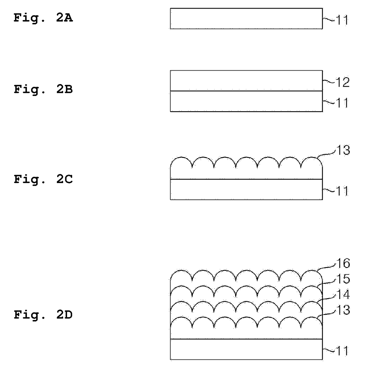
[0111]In Embodiment 2, the corrugated layer 24 was formed by forming the metal layer 23 over the entire polymer layer 22 formed on the substrate 21 and applying the ion bombardment stress and the heating stress thereto. However, the patterning process of patterning the polymer layer 22 formed on the substrate 21 may be further performed as in Modified Example 1 (FIG. 6C), and then the metal layer 23 may be formed so that a size thereof is matched with the size of the polymer layer 22 that is patterned to have a predetermined shape (FIG. 6D). Subsequent processes are the same as those of FIGS. 4D and 4E described in Embodiment 2.

[0112]Further, the reason to pattern the polymer layer 22 at a predetermined size is the same as described in Modified Example 1.

embodiment 3

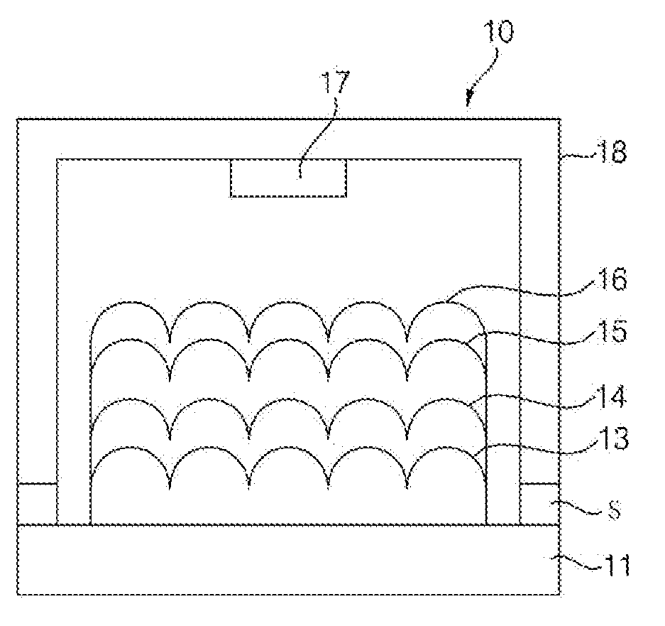
[0113]Next, preferred Embodiment 3 of the present invention will be described with reference to FIG. 12. FIG. 12 is a cross-sectional view illustrating an organic EL device according to preferred Embodiment 3 of the present invention.

[0114]Embodiment 3 is different from Embodiments 1 and 2, and Modified Examples 1 and 2 in that in the organic EL devices of Embodiments 1 and 2, and Modified Examples 1 and 2, the first electrode, the organic light-emitting layer, the second electrode, and the like are formed on the corrugated layer, but in Embodiment 3, the first electrode, the organic light-emitting layer, the second electrode, and the like are formed on a surface of the substrate opposite to a surface on which the corrugated layer is formed.

[0115]As illustrated in FIG. 12, in an organic EL device 30 of Embodiment 3, a first electrode 34, an organic light-emitting layer 35, and a second electrode 36 are sequentially formed on a surface of the substrate 31 opposite to the surface on w...


PUM

PropertyMeasurementUnit
thicknessaaaaaaaaaa
transmittanceaaaaaaaaaa
refractive indexaaaaaaaaaa

Abstract

The purpose of the present invention is to reduce light, which is absorbed at an interface of an organic electroluminescence device and disappears, thereby improving the efficiency of extraction of light that is drawn to the outside. A substrate 11 is coated with polymer to form a polymer layer 12; ion bombardment stress resulting from plasma is applied to the polymer layer 12 to form a corrugated layer 13 having a plurality of corrugated parts; and a first electrode, an organic light-emitting layer, and a second electrode are successively formed on the substrate, on which the corrugated layer is formed, thereby manufacturing an organic electroluminescence device. In addition, a metal layer 23 may be additionally formed on the polymer layer, ion bombardment stress and thermal stress may be applied simultaneously to form corrugated parts, and the metal layer may then be removed.

Description

TECHNICAL FIELD[0001]The present invention relates to a method for manufacturing a substrate, a method for manufacturing an organic electroluminescence device using the substrate, and a substrate and an organic electroluminescence device manufactured by the methods.BACKGROUND ART[0002]An organic electroluminescence device (hereinafter, briefly referred to as an organic EL device) is a light emitting device having a structure in which an organic light-emitting layer including an organic compound is inserted between a pair of electrodes which includes a cathode and an anode and is formed on a transparent substrate such as a glass substrate, etc., and holes and electrons are injected into the organic light-emitting layer from the pair of electrodes to recombine the holes and the electrons, thereby generating excitons, such that emission of light when activity of the excitons is lost is used to display, and the like.[0003]An organic electroluminescence display device using the organic E...

Claims


Application Information

Patent Timeline
Patent Type & Authority Applications(United States)
IPC IPC(8): H01L51/56H01L51/52
CPCH01L51/5268H01L51/56G02B5/021G02B5/0268G02B1/12H10K77/10H10K50/813H10K50/854H10K71/00
Inventor YOO, MIN-SANGIM, WOO-BINKIM, TAE-SU
Owner NEOVIEWKOLON
Why Eureka
Try Eureka