Protective film detecting method for laser processing

a technology of laser processing and protective film, which is applied in the direction of fluorescence/phosphorescence, instruments, semiconductor/solid-state device testing/measurement, etc., can solve the problems of reducing laser processing productivity, laser processing may be hindered by the protective film, and the wafer cannot be sufficiently protected, so as to accurately measure the thickness of the protective film and reduce laser processing productivity.

Active Publication Date: 2017-06-22
DISCO CORP
View PDF6 Cites 9 Cited by
  • Summary
  • Abstract
  • Description
  • Claims
  • Application Information

AI Technical Summary

Benefits of technology

[0006]However, in processing the semiconductor wafer through the protective film by using a laser beam, it is preferable to set the thickness of the protective film evenly to a predetermined value. That is, the thickness of the protective film has an effect on the result of laser processing. If the thickness of the protective film is less than the predetermined value, there is a possibility that the wafer cannot be sufficiently protected from the debris, whereas if the thickness of the protective film is greater than the predetermined value, there is a possibility that laser processing may be hindered by the protective film. It is therefore desired to accurately measure the thickness of the protective film formed on the semiconductor wafer before laser processing. Further, if much time is required for the measurement of the thickness of the protective film, the productivity in laser processing is reduced.
[0007]It is therefore an object of the present invention to provide a protective film detecting method which can accurately and simply detect the formed condition of a protective film formed on the front side of a workpiece.
[0010]According to the present invention, the protective film is formed of a water-soluble resin containing an absorbing agent. This protective film is formed on the front side of the workpiece, and the excitation light is applied to the protective film. At this time, the absorbing agent contained in the protective film absorbs the excitation light to emit fluorescence. Then, the intensity of this fluorescence is measured and it is determined whether or not the protective film has a desired thickness according to the fluorescence intensity measured above. Accordingly, the thickness of the protective film can be measured accurately and easily by using the excitation light having an absorption wavelength to the absorbing agent contained in the protective film. Further, as the excitation light for the detection of the protective film, continuous-wave light having a single wavelength is used. Accordingly, damage to the protective film due to the excitation light can be suppressed and it can be accurately determined whether or not the protective film has a desired thickness.

Problems solved by technology

If the thickness of the protective film is less than the predetermined value, there is a possibility that the wafer cannot be sufficiently protected from the debris, whereas if the thickness of the protective film is greater than the predetermined value, there is a possibility that laser processing may be hindered by the protective film.
Further, if much time is required for the measurement of the thickness of the protective film, the productivity in laser processing is reduced.

Method used


Image

  • Protective film detecting method for laser processing
  • Protective film detecting method for laser processing
  • Protective film detecting method for laser processing

Examples


Embodiment Construction

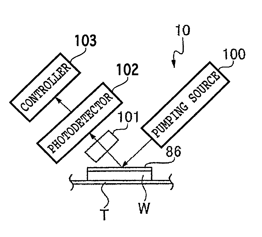
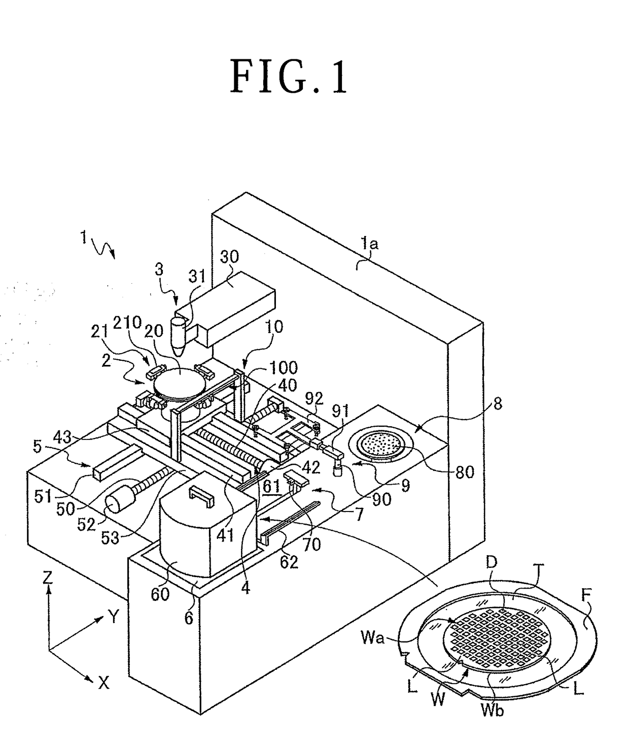
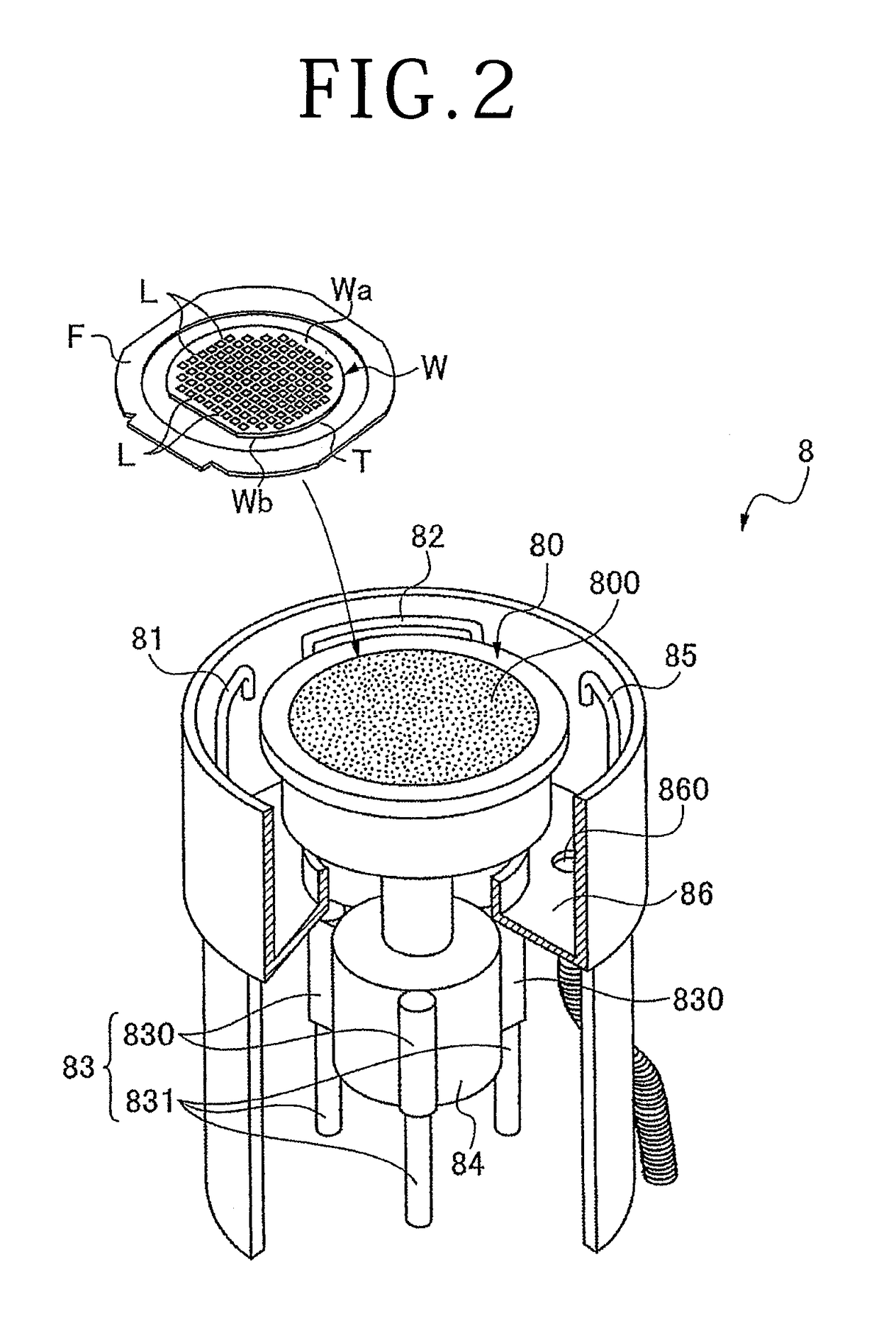
[0036]Referring to FIG. 1, there is shown a laser processing apparatus 1 for use in performing the present invention. The laser processing apparatus 1 shown in FIG. 1 has a function of forming a protective film on the front side Wa of a workpiece W, a function of determining whether or not the protective film formed has a desired thickness, and a function of laser-processing the workpiece W. The laser processing apparatus 1 includes a cassette mounting area 6 for mounting a cassette 60 storing the workpiece W as a target to be laser-processed, workpiece handling means 7 for handling the workpiece W to take it out of the cassette 60 before laser processing or store it into the cassette 60 after laser processing, protective film forming means 8 for forming a protective film on the front side Wa of the workpiece W taken out of the cassette 60, a chuck table 2 for holding the workpiece W on which the protective film has been formed, and laser beam applying means 3 for applying a laser b...


PUM

PropertyMeasurementUnit
wavelengthaaaaaaaaaa
peak wavelengthaaaaaaaaaa

Abstract

Disclosed herein is a protective film detecting method of detecting the formed condition of a protective film formed on the front side of a workpiece. The protective film detecting method includes a fluorescence intensity measuring step of forming a plurality of reference protective films having different thicknesses on the front sides of a plurality of reference workpieces, next applying excitation light absorbable by an absorbing agent contained in each reference protective film to each reference protective film, and next measuring the intensity of fluorescence emitted from the absorbing agent due to the absorption of the excitation light, and a threshold deciding step of deciding a threshold of the fluorescence intensity corresponding to a desired one of the different thicknesses of the reference protective films according to the fluorescence intensity measured above.

Description

BACKGROUND OF THE INVENTION[0001]Field of the Invention[0002]The present invention relates to a method of determining whether or not a protective film has a desired thickness, the protective film being formed on the front side of a workpiece such as a semiconductor wafer in dividing the workpiece by laser processing.[0003]Description of the Related Art[0004]As a method of dividing a workpiece such as a semiconductor wafer along streets (division lines), there is a method of laser-processing the workpiece along the streets to thereby divide the workpiece (see Japanese Patent Laid-open No. 1994-120334, for example). In the laser processing method described in Japanese Patent Laid-open No. 1994-120334, a laser beam is applied to the semiconductor wafer along the streets to generate thermal energy on the semiconductor wafer in an area corresponding to the streets, thereby continuously processing the semiconductor wafer in this area irradiated with the laser beam. There is a case that th...

Claims


Application Information

Patent Timeline
Patent Type & Authority Applications(United States)
IPC IPC(8): G01N21/64
CPCG03F7/70608H01L22/26G01N2021/6495H01L22/12G01N21/64C23C16/52H01L21/6836H01L22/20H01L2221/68327H01L2221/6834H01L21/67253G01N21/645G01N21/8422G01N2021/8427G01B11/0658H01L22/24H01L21/78H01L21/268
Inventor RYO, SENICHIOHURA, YUKINOBU
Owner DISCO CORP
Why Eureka
Try Eureka