Supercharge Your Innovation With Domain-Expert AI Agents!

Electrophoretic display device and electronic apparatus

a display device and display device technology, applied in non-linear optics, instruments, optics, etc., can solve the problems of inability to directly measure the resistance value of the contact resistor of a common electrode, and difficulty in manufacturing cost to use a method

Active Publication Date: 2017-06-22
E INK CORPORATION
View PDF3 Cites 3 Cited by
  • Summary
  • Abstract
  • Description
  • Claims
  • Application Information

AI Technical Summary

Benefits of technology

This patent talks about an electrophoretic display device and an electronic apparatus that can measure the resistance value of the common electrode. The device has multiple terminals that are connected to the common electrode, making it easier to connect the terminals. This feature allows for direct measurement of the resistance of the common electrode, which is important for the performance of the display. Ultimately, this technology simplifies the manufacturing process for electrophoretic display devices.

Problems solved by technology

Therefore, it would be difficult in terms of manufacturing cost to use a method of, as in a conventional semiconductor process, forming a through hole by etching and then sputtering metal such as AL (aluminum) for forming a contact for a common electrode.
In this structure, it is not possible to directly measure the resistance value of the contact resistor of the common electrode.
As explained above, in an electrophoretic display device according to related art, it is not possible to directly measure the resistance value of the contact resistor of a common electrode.
For example, in related art, there is a problem that a direct measurement approach cannot be taken; specifically, there is no option but to shave the periphery of a part of the common electrode so as to expose the contact portion of the common electrode, wire the exposed portion, and measure the resistance value of the contact resistor on the basis of the current value of the wiring indirectly.

Method used


Image

  • Electrophoretic display device and electronic apparatus
  • Electrophoretic display device and electronic apparatus
  • Electrophoretic display device and electronic apparatus

Examples


first embodiment

Overview of Contact Structure of COM Electrode

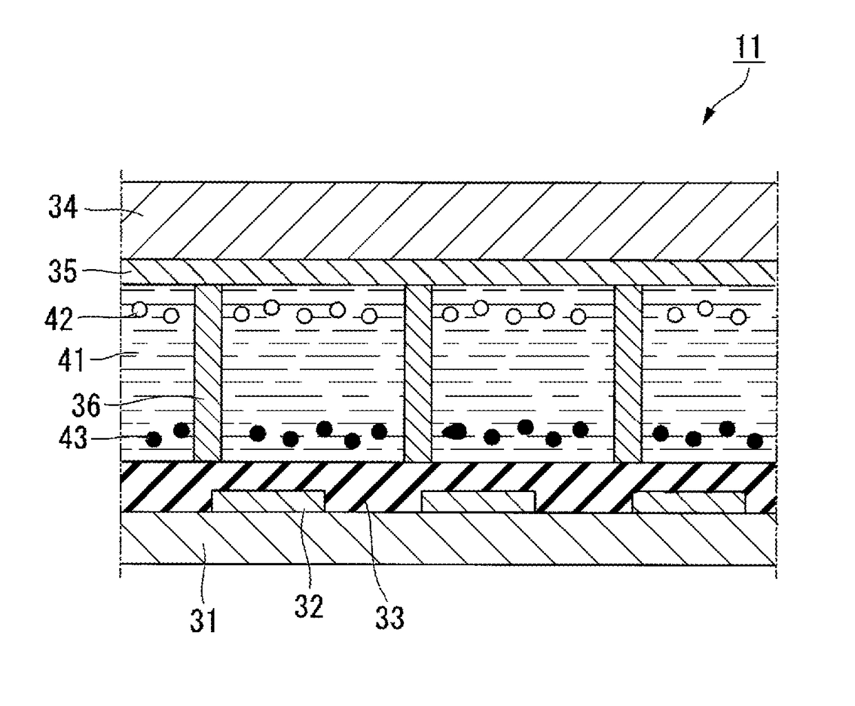
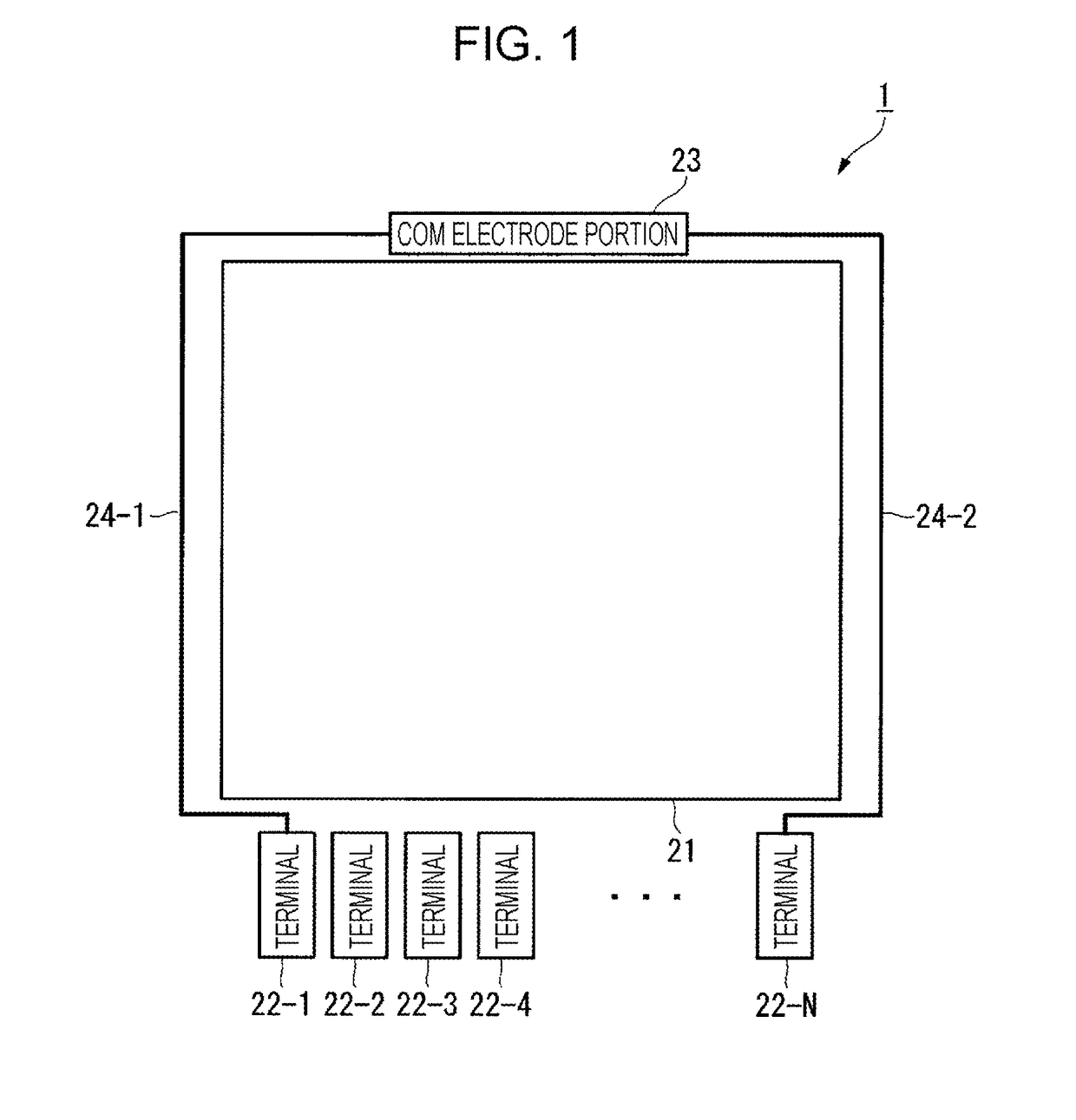
[0036]FIG. 1 is a diagram that illustrates an example of the contact structure 1 of COM electrodes of an electrophoretic display device according to an exemplary embodiment (first embodiment) of the invention. The pixel area portion 21 of a pixel substrate, plural terminals whose number is N (where N is an integer that is greater than one and may be the same as M shown in FIG. 13; denoted as 22-1 to 22-N), wiring lines 24-1 and 24-2, and a COM electrode portion 23 are shown in FIG. 1. In the present embodiment, the terminals located at both ends (terminals 22-1 and 22-N) are at the same potential when driven. One terminal 22-1 is connected to the COM electrode portion 23 via the wiring line 24-1. Another terminal 22-N is connected to the COM electrode portion 23 via the other wiring line, that is, 24-2. The COM electrode portion 23 is connected to the common electrode of the opposite substrate (not illustrated in FIG. 1). As described ab...

second embodiment

[0064]Next, with reference to FIGS. 10, 11, and 12, a second embodiment will now be explained. Structure examples of an electronic apparatus according to an exemplary embodiment of the invention are illustrated in these drawings. The following description of the present embodiment shows specific examples of an electronic apparatus to which an electrophoretic display device according to the foregoing embodiment (electrophoretic display device according to the first embodiment) is applied.

[0065]FIG. 10 is a diagram that schematically illustrates a structure example of an electronic apparatus according to an exemplary embodiment (first example of the second embodiment) of the invention. More specifically, FIG. 10 is a perspective view of an electronic book 501 that is an example of an electronic apparatus. The electronic book 501 includes a book frame 511, a display unit 512, and an operation unit 513. An electrophoretic display device according to the foregoing embodiment is applied t...


PUM

PropertyMeasurementUnit
heightaaaaaaaaaa
heightaaaaaaaaaa
electric fieldaaaaaaaaaa

Abstract

An electrophoretic display device includes: a first substrate on which a common electrode is provided; a second substrate on which a pixel electrode and a plurality of terminals are provided; dispersion liquid that is provided between the first substrate and the second substrate and includes particles and a dispersion medium; and two or more connecting portions that electrically connect two or more terminals among the plurality of terminals respectively to different points of the common electrode.

Description

BACKGROUND[0001]1. Technical Field[0002]The present invention relates to an electrophoretic display device and an electronic apparatus.[0003]2. Related Art[0004]A display device using electrophoresis (electrophoretic display device) is known. An electrophoretic display device has an electrophoretic layer between two substrates facing each other (in this specification, these two substrates are referred to as “pixel substrate” and “opposite substrate”), and performs display by utilizing the motion, under the influence of an electric field, of charged particles (migration particles) that migrate in a dispersion medium (solvent) that exists in the electrophoretic layer. The electric field is generated by applying a potential difference between the two substrates. A surface of one of the two substrates (surface of the opposite substrate) is a display surface. A partitioning wall is provided between the two substrates. The electrophoretic layer is compartmentalized by the partitioning wal...

Claims


Application Information

Patent Timeline
Patent Type & Authority Applications(United States)
IPC IPC(8): G02F1/167G02F1/1676
CPCG02F1/167G02F2001/1676G02F2001/1672G02F2201/121G02F1/1676G02F1/1681
Inventor MATSUMOTO, AKIHITO
Owner E INK CORPORATION
Features
  • R&D
  • Intellectual Property
  • Life Sciences
  • Materials
  • Tech Scout
  • Unparalleled Data Quality
  • Higher Quality Content
  • 60% Fewer Hallucinations
Learn More