Inter-Chip Alignment

a technology of inter-chips and waveguides, applied in the field of microchips, can solve the problems of inability to create various components of a sensing system from the same material, inability to cost-effectively integrate a waveguide and a detector on it, and inability to optimize the quality of detectors, etc., to achieve the effect of reducing the inter-chip spacing, reducing the coupling loss of waveguide and waveguide, and improving the coupling loss

Active Publication Date: 2017-06-22
UNIV OF NOTRE DAME DU LAC +1
View PDF5 Cites 8 Cited by
  • Summary
  • Abstract
  • Description
  • Claims
  • Application Information

AI Technical Summary

Benefits of technology

[0011]In accordance with the present invention, optical quilt packaging is implemented for chip-to-chip integration of photonic devices such as laser, waveguide and photodetector devices. For compact low cost on chip mid infrared detection using a QC laser, it is important that wafer materials different from that used for the QC laser be employed for the waveguide and detector. In accordance with one aspect of the present invention, quilt packaging is employed to integrate the chips after separately fabricating them. Using quilt packaging it is possible to integrate widely different wavelength QC lasers, waveguides made on a comparably low cost wafers (silicon on insulator, SOI) and better detectors for low cost, improved quality liquid phase detection.
[0012]On chip integration of a quantum cascade (QC) laser with waveguide and detector is already reported [1], but to obtain greater flexibility in laser operating wavelength and better quality detection, chip to chip optical integration still has a long way to go. The quilt packaging approach of the present invention can be a good solution for chip-to-chip optical integration as different material wafers could be used in the fabrication of QC lasers, waveguides and detectors, providing both reduced cost and high performance application.
[0014]According to another aspect of the present invention, the depth of the notches and length of the nodules can be selected to control the inter-chip distance. Making the notches deeper than the length of the nodules can be used to reduce the inter-chip spacing to reduce the waveguide-waveguide coupling loss. The inter-chip gap can also be filled with an index matching material to improve the coupling loss or flowing a liquid in the channel formed by the inter-chip gap can change the optical properties of the interconnect, and allow analysis of the fluid. The nodules and notches can also be metalized to allow for permanently connecting them together by, for example, soldering, and / or to provide a high bandwidth electrical connection between the two chips that can be used for chip / component input / output. The process of the present invention minimizes the changes to conventional processing of the individual components and is thus is easily integrated into conventional semiconductor processes, maintains electrical continuity across several chips, and scales with high volume production.
[0015]In conventional quilt packaging techniques conductive nodules protruding from the sides of ICs provide means of a direct edge-to-edge interconnection between the ICs in a quilt-like fashion. In optical quilt packaging it is not always necessary to exchange electrical signals between the ICs, the present invention employs using the nodules and nodules and notches as a mean of alignment between the waveguides of different chips. In the proposed optical quilt packaging, optical transmission between the emitters, detectors, and waveguides of different chips would make the effective photonic device integration.

Problems solved by technology

But since the QC laser wafer is very expensive, integrating a waveguide and detector on it is not cost effective and at the same time the detector quality is not optimized.
Unfortunately, quite often the various components of a sensing system cannot all be created from the same material because of physical limitations and costs.

Method used


Image

  • Inter-Chip Alignment
  • Inter-Chip Alignment
  • Inter-Chip Alignment

Examples


Embodiment Construction

[0023]Persons of ordinary skill in the art will realize that the following description of the present invention is illustrative only and not in any way limiting. Other embodiments of the invention will readily suggest themselves to such skilled persons.

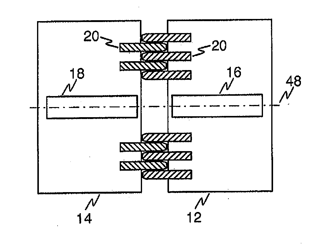
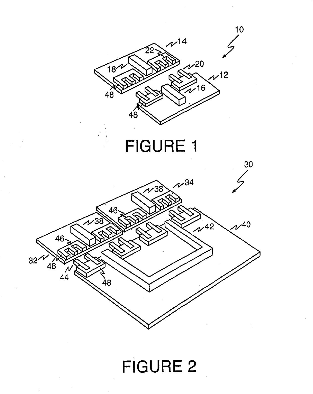
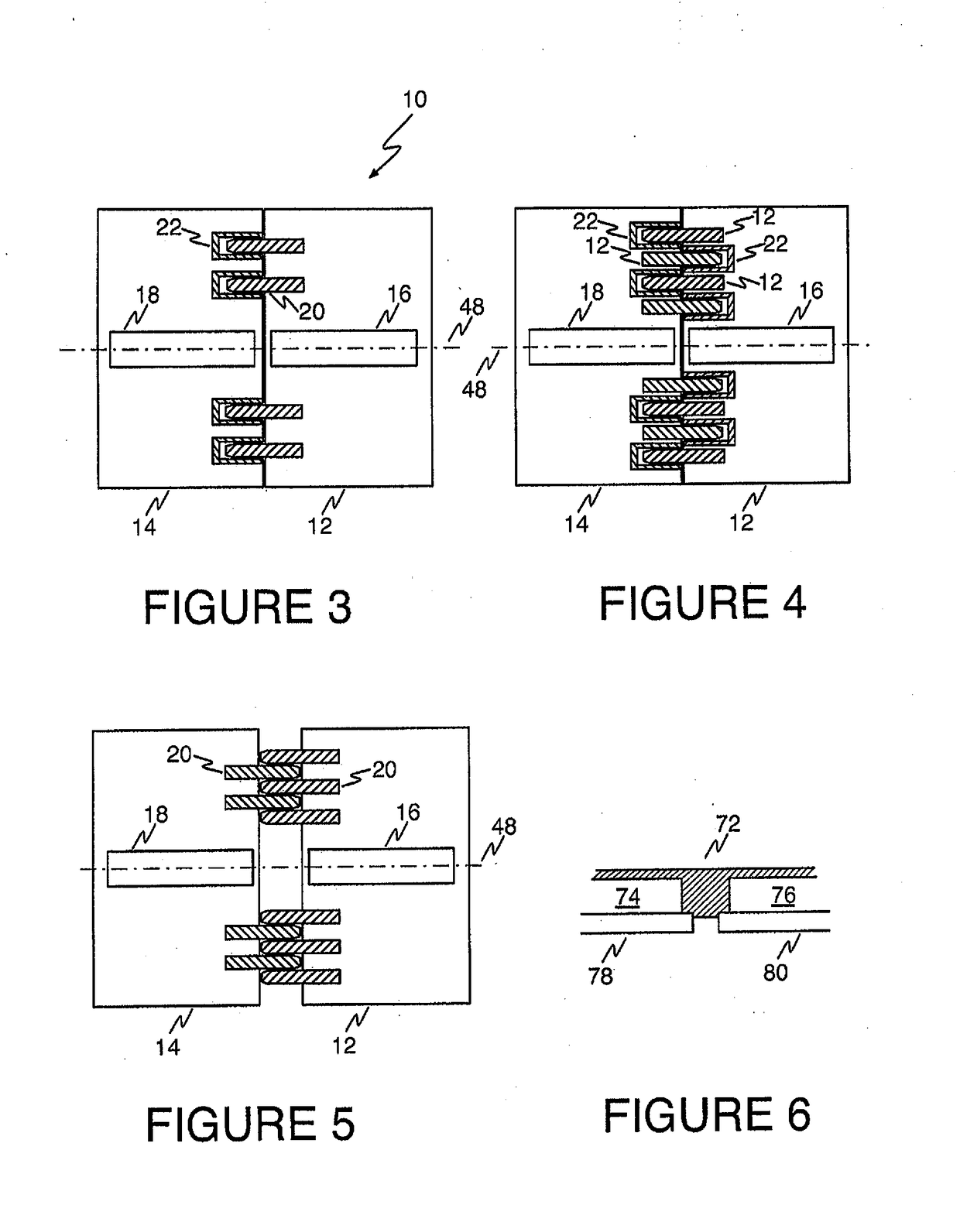
[0024]Referring first to FIG. 1, an isometric drawing shows how two optical components on two different integrated circuit chips can be optically coupled to one another using the teachings of the present invention. An assembly 10 is formed from a first integrated circuit chip 12 and a second integrated circuit chip 14. First integrated circuit chip 12 includes a first optical component 16 disposed on it. Optical component 16 may be an emitter, such as an integrated circuit laser, a detector, or a waveguide. Similarly, second integrated circuit chip 14 includes a second optical component 18 disposed on it. Optical component 18 may be an emitter, such as an integrated circuit laser, a detector, or a waveguide.

[0025]Integrated circuit ch...


PUM


Abstract

First and second integrated devices each have an optical component and a plurality of interconnect structures disposed one edge thereon. The first edge surface of the second integrated device is positioned contiguous to the first edge surface of the first integrated device. The interconnect structures disposed on the first integrated device are in physical contact with the interconnect structures disposed on the edge surface of the second integrated device so as to provide alignment for conveying at least one signal between the optical components on the first and second integrated devices.

Description

CROSS REFERENCE TO RELATED APPLICATIONS[0001]This application is a continuation of U.S. patent application Ser. No. 14 / 158,079, filed Jan. 17, 2014 which claims the benefit of U.S. Provisional Patent Application No. 61 / 849,090, filed Jan. 18, 2013, both of which are incorporated herein by reference in their entirety.BACKGROUND OF THE INVENTION[0002]Field of the Invention[0003]The present invention relates generally to microchips and systems and devices employing microchips.[0004]Description of Related Art[0005]Quilt packaging is a new paradigm for inter-chip electrical communication. In quilt packaging conducting nodules that protrude from the vertical facets of integrated circuits are used for a dense, enhanced speed, and reduced-power interface between multiple dies within a package. See, e.g., G. H. Bernstein, Q. Liu, Z. Sun, and P. Fay, Quilt-packaging: a new paradigm for inter-chip communication; Proc. IEEE 7th Electronics Packaging Technology Conference, 2005, pp. 1-6; U.S. Pa...

Claims


Application Information

Patent Timeline
Patent Type & Authority Applications(United States)
IPC IPC(8): H01L25/16H01L23/00H01L21/66
CPCH01L25/167H01L22/12H01L2224/1718H01L2224/175H01L24/17G02B6/423G02B6/4238G02B6/4257H01L24/70
Inventor HALL, DOUGLAS C.HOWARD, SCOTTHOFFMAN, ANTHONYBERNSTEIN, GARY H.KULICK, JASON M.
Owner UNIV OF NOTRE DAME DU LAC
Why Eureka
Try Eureka