Array substrate and manufacturing method for the same

Active Publication Date: 2017-06-29
TCL CHINA STAR OPTOELECTRONICS TECH CO LTD
View PDF0 Cites 1 Cited by
  • Summary
  • Abstract
  • Description
  • Claims
  • Application Information

AI Technical Summary

Benefits of technology

[0020]The beneficial effect of the present invention is: in the array substrate and the manufacturing method of the present, through patterning the first metal layer through a first mask to form a gate electrode and a first conductive layer which are disposed at an interval; patterning the semiconductor layer and the gate insulation layer through a second mask to form a through hole for revealing the first conductive layer; patterning the semiconductor layer through the gate electrode and the first conductive layer to form a first channel region and a second channel region which are disposed at an interval;

Problems solved by technology

In the manufacturing process of the array substrate, two different masks are required to respectively patterning a

Method used


Image

  • Array substrate and manufacturing method for the same
  • Array substrate and manufacturing method for the same
  • Array substrate and manufacturing method for the same

Examples


Example

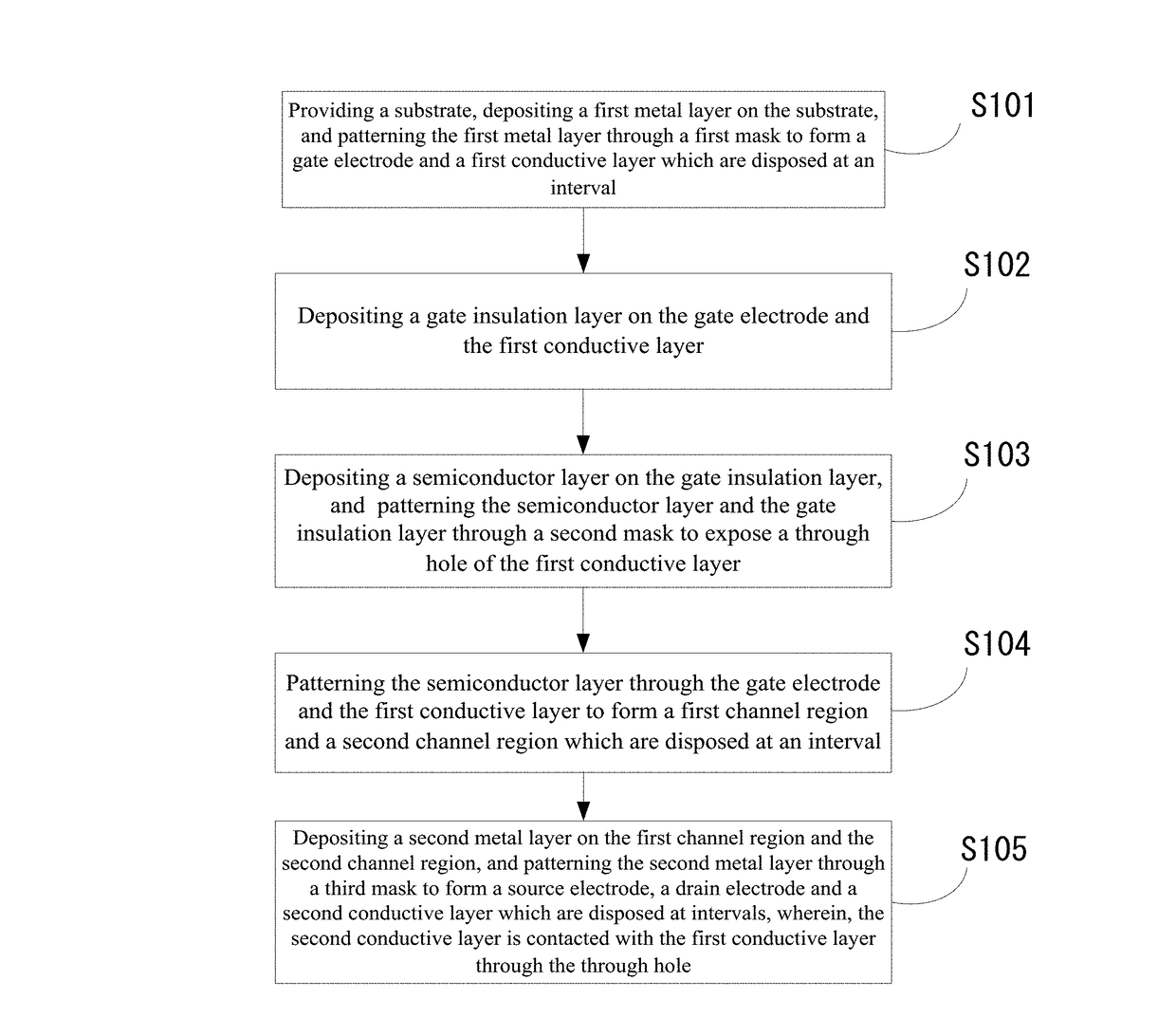
[0024]In the embodiment and claims of the present invention, some vocabularies are used to indicate some specific elements. A person skilled in the art can understand that manufacturers may use a different vocabulary to indicate a same element. The present embodiment and claims do not use the difference in the vocabularies to distinguish the elements. The present embodiment and claims utilize the difference in the functions of the elements to distinguish the elements. The following content combines with the drawings and the embodiment for describing the present invention in detail.

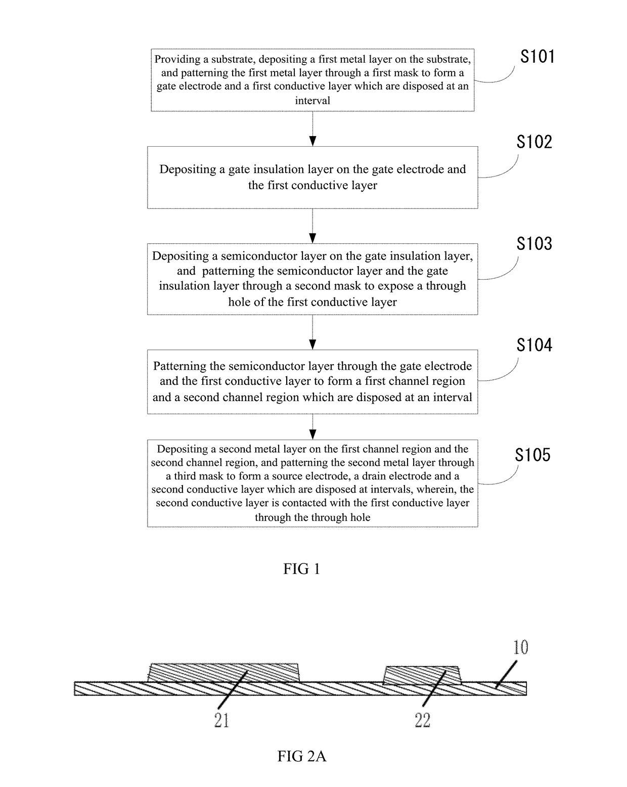
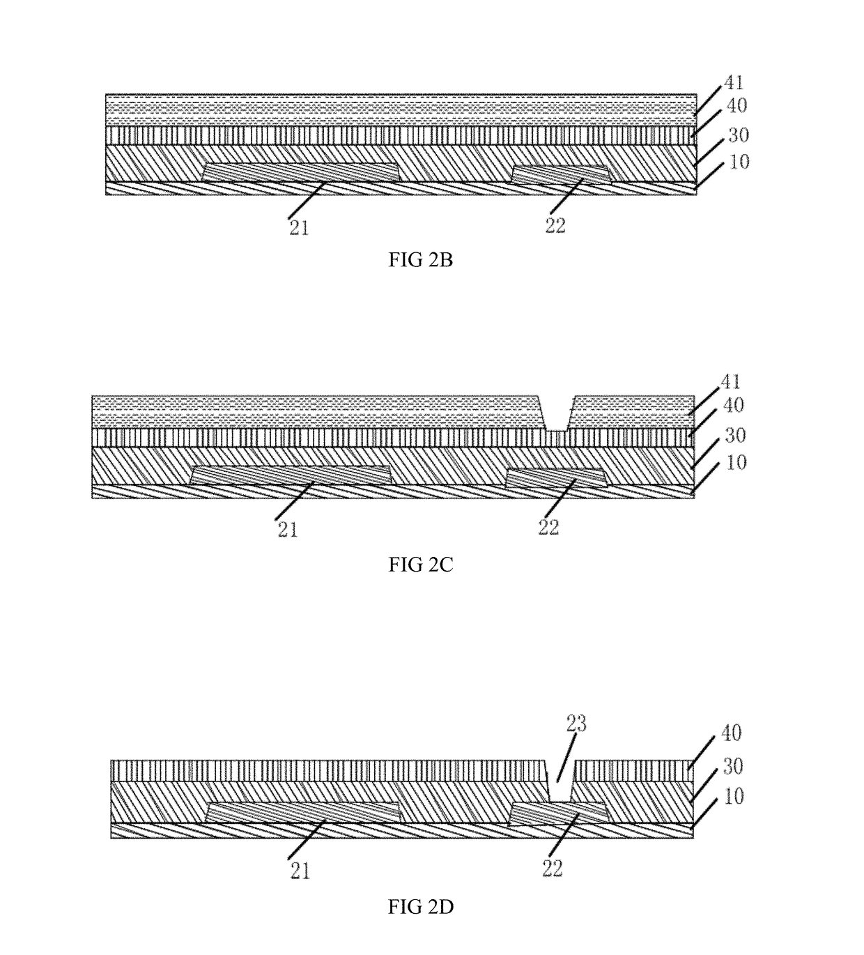
[0025]FIG. 1 is a flowchart of a manufacturing method for an array substrate according to an embodiment of the present invention; FIG. 2A-2G is a schematic structure diagram for an array substrate in the manufacturing process of the manufacturing method shown in FIG. 1. It should be noted that if there exists a substantially same result, the method of the present invention is not limited to the flowchart s...


PUM


Abstract

An array substrate and a manufacturing method therefor. The method comprises: patterning a first metal layer by means of a first photomask so as to form a gate electrode (21) and a first conductor (22) which are arranged at an interval; patterning a semiconductor layer (40) and a gate insulating layer (30) by means of a second photomask so as to form a through hole (23) which Is exposed out of the first conductor (22); patterning the semiconductor layer (40) by means of the gate electrode (21) and the first conductor (22) so as to form a first channel region (43) and a second channel region (44) which are arranged at an interval; and patterning a second metal layer by means of a third photomask so as to form a source electrode (51), a drain electrode (52) and a second conductor (53) which are arranged at intervals, wherein the second conductor (53) is in contact with the first conductor (22) via the through hole (23). By means of the manufacturing method for the array substrate, the semiconductor layer (40) and the gate insulating layer (30) are patterned by means of a photomask, so that the production costs of the array substrate are reduced, bridging between the first conductor (22) and the second conductor (53) is realized using a relatively simple method, and the production efficiency of the array substrate is further improved.

Description

BACKGROUND OF THE INVENTION[0001]1. Field of the Invention[0002]The present invention relates to a liquid crystal field, and more particularly to an array substrate and a manufacturing method for the same.[0003]2. Description of Related Art[0004]In an Active Matrix Liquid Crystal Display (AMLCD) or an Active-matrix organic light emitting diode (AMOLED) display, a Gate Driver on Array (GOA) technology is utilized to achieve a narrow-frame effect.[0005]Wherein, in the GOA technology, in the manufacturing process for an array substrate, two metal layers disposed separately are required. At the same time, the two metal layers have to cross a gate insulation layer of the array substrate for connecting. Therefore, how to connecting the two metal layers by a relative simple way in order to improve the production efficiency is an urgent problem need to be solved. Besides, in order to realize connecting of the two metal layers. In the manufacturing process of the array substrate, two differe...

Claims


Application Information

Patent Timeline
IPC IPC(8): H01L21/8234H01L21/027G02F1/1333H01L21/033
CPCH01L21/823462H01L21/0331G02F2001/1635G02F1/1333H01L21/0272H01L21/77H01L27/12H01L27/124H01L27/1288H01L21/84H01L2021/775H01L23/52
Inventor SHI, LONGQIANG
Owner TCL CHINA STAR OPTOELECTRONICS TECH CO LTD
Why Eureka
Try Eureka