Advanced Control Circuit for Switched-Mode DC-DC Converter

Inactive Publication Date: 2017-07-06
TEXAS INSTR INC
14 Cites 3 Cited by

AI-Extracted Technical Summary

Problems solved by technology

As the operating frequency of the switching regulator circuit of FIG. 2A increases, several problems limit circuit efficiency.
Due to noise or other effects, reference voltage VREF can be subject to error such that output voltage VOUT is compared to VREF′, t...

Benefits of technology

[0022]FIG. 7 is a schematic diagram ...

Abstract

A voltage converter (FIG. 4) for a power supply circuit is disclosed. The voltage converter comprises a control circuit (400) coupled to receive an enable (EN) signal. The control circuit produces a first control signal (PWM) to provide a load current (IL) in response to the enable signal. A sample and hold circuit (408) is arranged to produce a third control signal (CSP) to emulate the load current and a fourth control signal (CSN′) to sample and hold value of the third control signal. A comparator circuit (416) is arranged to compare the third and fourth control signals and produce the enable signal in response to a result of the comparison.

Application Domain

Efficient power electronics conversionDc-dc conversion +1

Technology Topic

Comparators circuitsVoltage converter +6

Image

  • Advanced Control Circuit for Switched-Mode DC-DC Converter
  • Advanced Control Circuit for Switched-Mode DC-DC Converter
  • Advanced Control Circuit for Switched-Mode DC-DC Converter

Examples

  • Experimental program(1)

Example

[0023]The preferred embodiments of the present invention provide significant advantages over DC-DC voltage converters of the prior art as will become evident from the following detailed description.
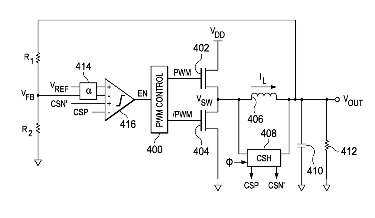
[0024]Referring to FIG. 4, there is a DC-DC voltage regulator circuit of the present invention. Here and in the following discussion, the same reference numerals are used in various drawing figures to indicate the same circuit elements. The voltage regulator includes a pulse width modulation (PWM) control circuit 400 that produces control signal PWM and complementary control signal /PWM. In some embodiments of the present invention, complementary control signal /PWM may be omitted. N-channel transistor 402 has a current path coupled between supply voltage VDD and voltage terminal VSW controlled by PWM. N-channel transistor 404 has a current path coupled between voltage terminal VSW and reference supply voltage terminal VSS. The current path of n-channel transistor 404 is controlled by /PWM. Inductor 406 is coupled between voltage terminal VSW and output terminal VOUT to supply load current IL to load capacitance 410 and load resistance 412. A current sample and hold circuit 408 is coupled in parallel with inductor 406 and produces control signals CSP and CSN′ as will be explained in detail.
[0025]Output voltage VOUT is fed back to a voltage divider formed by resistors R1 and R2 to produce feedback voltage VFB at their common terminal. Feedback voltage VFB is compared with reference voltage VREF and CSP is compared with CSN′ by comparator circuit 416 to produce enable signal EN. The comparison of VFB with VREF has a gain factor a (414) relative to the comparison of CSP and CSN′. In a preferred embodiment of the present invention, gain factor α has a value of 4 as determined by relative conductivity of comparator transistors.
[0026]Turning now to FIG. 5A, current sample and hold circuit 408 will be described in detail. Resistor 500 and capacitor 502 are connected in series between voltage terminal VSW and output terminal VOUT to form an RC filter. Control signal CSP emulates the current through inductor 406. Here, emulate means minimum and maximum values of CSP occur at substantially the same time as minimum and maximum values of IL, respectively. Moreover, CSP increases as IL increases. A first buffer (BUF1) applies CSP to resistor 512 and to switches controlled by clock signals Φ1 and Φ2. Here and in the following discussion, switches are used by way of explanation. In preferred embodiments of the present invention these switches may be bipolar transistors, MOS transistors, CMOS transmission gates, or other devices that are well known in the art. A switch controlled by clock signal Φ3 selectively connects resistor 512 to the input terminal of a second buffer (BUF2). Capacitor 506 is coupled to receive and store buffered signal CSP (VC1) when the switch controlled by clock signal Φ1 is closed. Likewise, capacitor 508 is coupled to receive and store buffered signal CSP (VC2) when the switch controlled by clock signal Φ2 is closed. Clock signals Φ1 and t2 are alternately activated to apply one of VC1 and VC2 to the input terminal of buffer BUF2 when Φ2 and Φ1 are activated, respectively. Buffer BUF2 applies the respective sampled CSP (VC1 or VC2) to capacitor 504 via resistor 510 where it is stored as CSN′.
[0027]Referring now to FIG. 5B, operation of the circuit to generate clock signals Φ1, Φ2, and Φ3 for the circuit of FIG. 5A will be described in detail. Pull up (PU) and pull down (PD) control signals are generated by the PWM control circuit of FIG. 7 and correspond to control signals PWM and /PWM as will be described in detail. Delay flip flop 520 is coupled to receive control signal PU at a clock terminal and produces a high level of clock signal Φ1 at a first time. Inverter 522 responsively produces a complementary low level of clock signal Φ2 at the first time. The complementary output (/Q) of delay flip flop 520 is coupled to input terminal D so that a next high level of control signal PU at the clock terminal and produces a low level of clock signal Φ1 at a second time. Inverter 522 responsively produces a complementary high level of clock signal Φ2 at the second time.
[0028]In a discontinuous operating mode (DCM), control signals PU and PD are both low at the same time. NOR gate 524 produces a high level signal at the input of a delay inverter formed by p-channel transistor 526, n-channel transistor 528, and an intermediate resistor. The output of the delay inverter is coupled to capacitor 532 to provide an RC output delay. Inverter 530 is coupled to receive the output signal from the delay inverter and produce a high level of clock signal Φ3 while PU and PD are both low. The delay inverter and RC elements are preferably designed to provide adequate time for PU and PD to settle so that CSP and CSN′ are approximately equal.
[0029]Turning now to FIG. 5C, continuous current mode (CCM) of the circuits of FIGS. 5A and 5B will be described in detail. At time t1, signal VSW (FIG. 4) goes high in response to control signal PU and corresponding signal PWM. Inductor current IL increases to a peak value at time t2 while VSW is high. Clock signal Φ1 also goes high at time t1 while clock signal Φ2 remains low. CSP emulates inductor current IL and attains a peak value at time t2. Since clock signal Φ1 is high, VC1 tracks CSP. CSN′ and VC2 remain low at a previously sampled value of CSP stored on capacitor 508. At time t2, PU and PWM go low and PD and /PWM go high. Responsively, load current IL decreases to a minimum value at time t3. CSP again emulates inductor current IL and attains a minimum value at time t3. Since clock signal Φ1 is high until time t3, VC1 tracks CSP. At time t3, clock signals Φ1 and 02 go low and high, respectively. The low level of Φ1 stores a minimum value of CSP on capacitor 506 and disconnects capacitor 508 from BUF2. The high level of Φ2 connects capacitor 506 to BUF2 and stores a new minimum value of CSP (VC2) on capacitor 508.
[0030]At time t3, signal VSW goes high again in response to control signal PU and corresponding signal PWM. Inductor current IL increases to a peak value at time t4 while VSW is high. Clock signal Φ2 goes high at time t3 while clock signal Φ1 remains low. CSP emulates inductor current IL and attains a peak value at time t4. Since clock signal Φ2 is high, VC2 tracks CSP. CSN′ and VC1 remain low at a previously sampled value of CSP stored on capacitor 506. At time t4, PU and PWM go low and PD and /PWM go high. Responsively, load current IL decreases to a minimum value at time t5. CSP again emulates inductor current IL and attains a minimum value at time t5. Since clock signal Φ2 is high until time t5, VC2 tracks CSP. At time t5, clock signals Φ1 and Φ2 go high and low, respectively. The low level of Φ2 stores a new minimum value of CSP (VC2) on capacitor 508 and disconnects capacitor 506 from BUF2. The high level of Φ1 connects capacitor 508 to BUF2 and stores a new minimum value of CSP (VC1) on capacitor 506. The foregoing sequence continues so that one of transistor 402 or 404 is on and the other is off
[0031]Referring next FIG. 5D, discontinuous current mode (DCM) of the circuits of FIGS. 5A and 5B will be described in detail. At time t1, signal VSW (FIG. 4) goes high in response to control signal PU and corresponding signal PWM. Inductor current IL increases to a peak value at time t2 while VSW is high. Clock signal Φ1 also goes high at time t1 while clock signals Φ2 and Φ3 remain low. CSP emulates inductor current IL and attains a peak value at time t2. Since clock signal Φ1 is high, VC1 tracks CSP. CSN′ and VC2 remain low at a previously sampled value of CSP stored on capacitor 508. At time t2, PU and PWM go low and PD and /PWM go high. Responsively, load current IL decreases to a minimum value at time t3. CSP again emulates inductor current IL and attains a minimum value at time t3. Since clock signal Φ1 is high, VC1 tracks CSP. At time t3, PD and /PWM go low and PU and PWM remain low. Clock signals Φ1 and Φ2 remain high and low, respectively. The low level of PU and PD at the input terminals of NOR gate 524 produces a high level output signal that is buffered by the delay inverter (526 and 528) and inverter 530 to produce a high level of clock signal Φ3. From time t3 until time t4, inductor current remains near zero and VSW is approximately equal to \Tour. Clock signal Φ3 remains high and connects the output of BUF1 to the input of BUF2 via resistor 512. Between t3 and t4, therefore, the present value of CSP replaces the previously sampled value (VC2) on capacitor 508. Responsively, BUF2 produces CSN′ as the present value of CSP. This advantageously avoids leakage of a stored CSP sample on capacitor 508 and maintains CSN′ equal to CSP for any time period from t3 to t4.
[0032]At time t4, signal VSW goes high again in response to control signal PU and corresponding signal PWM. The high level of PU drives clock signal Φ3 low to disconnect the output of BUF1 from the input of BUF2. Inductor current IL increases to a peak value at time t5 while VSW is high. Clock signal Φ2 goes high at time t4 and clock signal Φ1 goes low. CSP emulates inductor current IL and attains a peak value at time t5. Since clock signal Φ2 is high, VC2 tracks CSP. CSN′ and VC1 remain low at a previously sampled value of CSP stored on capacitor 506. At time t5, PU and PWM go low and PD and /PWM go high. Responsively, load current IL decreases to a minimum value at time t6. CSP again emulates inductor current IL and attains a minimum value at time t6. Since clock signal Φ2 is high until time t6, VC2 tracks CSP. The foregoing sequence may continue in DCM or transition to CCM in response to varying load conditions.
[0033]Referring now to FIG. 6, the 4-input comparator circuit 416 of FIG. 4 will be described in detail. In a preferred embodiment of the present invention, the 4-input comparator circuit includes five comparators 600-608. Comparator 600 compares reference voltage VREF to feedback voltage VFB. Comparator 602 compares CSN′ to CSP. As previously discussed, comparator 600 has a gain factor a greater than the gain of comparator 602. This gain factor is achieved by increasing the conductivity of transistors MP1 and MP2 with respect to transistors MP3 and MP4. Series connected comparators 604 and 606 amplify the combined difference voltage developed by comparators 600 and 602. Comparator 608 further amplifies the difference voltage from comparator 606 and applies a single output signal to inverter 610. Inverter 610 buffers the single output and produces enable signal EN, which is applied to PWM control circuit 400.
[0034]In operation, enable signal EN goes high when the common drain terminal (A) of transistors MP2 and MP4 is positive with respect to the common drain terminal (B) of transistors MP1 and MP3. This condition may occur when feedback voltage VFB is less than reference voltage VREF or when current sense signal CSP is less than current sense signal CSN′. A low-to-high transition of enable signal EN initiates a new on-time pulse in the PWM control circuit of FIG. 7 as will be explained in detail.
[0035]Referring to FIG. 7, there is a simplified schematic diagram of the PWM control circuit of FIG. 4. The PWM control circuit includes four major parts that will be discussed separately as well as control logic. First, the on-time timer section includes comparator 708, current source 710, capacitor 712, and n-channel transistor 714. N-channel transistor 714 initially discharges capacitor 712 while current source 710 is off. At the beginning of an on-time pulse, n-channel transistor 714 is turned off and current source 710 is turned on. Duration of the on-time pulse is determined by the time required for current source 710 to charge capacitor 712. Comparator 708 compares the voltage on capacitor 712 with output voltage VOUT. When the voltage on capacitor 712 exceeds output voltage VOUT, comparator 708 produces a high level output signal at the reset terminal of SR flip flop 702. This resets SR flip flop 702 and produces a low output signal at the Q terminal, thereby terminating the on-time pulse.
[0036]Second, the off-time timer section includes comparator 722, reference voltage source 724, current source 716, capacitor 718, and n-channel transistor 720. N-channel transistor 720 initially discharges capacitor 718 while current source 716 is off. At the beginning of an off-time pulse, n-channel transistor 720 is turned off and current source 716 is turned on. Duration of the off-time pulse is determined by the time required for current source 716 to charge capacitor 718. Comparator 722 compares the voltage on capacitor 718 with reference voltage source 724. When the voltage on capacitor 718 exceeds reference voltage source 724, comparator 722 produces a high level output signal at one input terminal of OR gate 728. The other input of OR gate 728 is still low as determined by the Q output of SR flip flop 702 in the previous on-time period. The high level output from OR gate 728 is applied to one input of AND gate 700. However, the next on-time pulse will not begin until enable signal EN goes high. The high level output from OR gate 728 is applied to inverter 730 to drive the S terminal of SR flip flop 734 low. The high level output from OR gate 728 is also applied to AND gate 732 to drive the R terminal of SR flip flop 734 high. The high level of the reset terminal of SR flip flop 734 produces a low output signal at the Q terminal, thereby terminating the off-time pulse.
[0037]Third, the zero crossing section includes comparator 740 and switch SWZC. The Q output of SR flip flop 734 is high during an off-time pulse, thereby producing a high level of PD and /PWM so that n-channel transistor 404 (FIG. 4) is on. The high level of the Q output of SR flip flop 734 activates switch SWZC so that comparator 740 compares voltage VSW to reference voltage VSS or ground. If voltage VSW goes negative with respect to ground during the off-time period, comparator 740 produces a low level output at an input of OR gate 726. Together with the low level from the Q terminal of SR flip flop 702, OR gate 726 produces a low level at an input of AND gate 732 to produce a low level at the R input of SR flip flop 734. The low level of the R input of SR flip flop 734 prevents termination of the off-time pulse even if the off-time timer has expired. Thus, n-channel transistor 404 remains on while voltage VSW is negative with respect to ground to prevent any significant undershoot that might induce minority carrier injection.
[0038]Fourth, the cross-conduction control section includes AND gates 704 and 736, buffers 706 and 738, comparators 742 and 744, and reference voltage sources 746 and 748. The cross-conduction control section assures that n-channel transistors 402 and 404 are never on at the same time. During an on-time period, for example, AND gate 704 produces a high level signal PU. Buffer 706 buffers this signal to provide a high level of PWM at the gate of n-channel transistor 402 as well as at one input of comparator 742. While the level of PWM exceeds reference voltage 746, comparator 742 produces a low level output that turns off n-channel transistor 714 and produces a low level signal PD and buffered signal /PWM. Thus, PD and /PWM remain low while PWM is greater than reference voltage 746. Likewise, during an off-time period AND gate 736 produces a high level signal PD. Buffer 738 buffers this signal to provide a high level of /PWM at the gate of n-channel transistor 404 as well as at one input of comparator 744. While the level of /PWM exceeds reference voltage 748, comparator 744 produces a low level output which, in turn, produces a low level signal PU and buffered signal PWM. Thus, PU and PWM remain low while /PWM is greater than reference voltage748.
[0039]Still further, while numerous examples have thus been provided, one skilled in the art should recognize that various modifications, substitutions, or alterations may be made to the described embodiments while still falling within the inventive scope as defined by the following claims. For example, although the previous on-time and off-time circuits disclose current ramps having a positive slope, alternative embodiments of the present invention may also employ current ramps having a negative slope or a combination of positive and negative slopes. Moreover, although embodiments of the present invention disclose a positive power supply voltage, other embodiments of the present invention may also be directed to a negative power supply voltage. Other combinations will be readily apparent to one of ordinary skill in the art having access to the instant specification.

PUM

no PUM

Description & Claims & Application Information

We can also present the details of the Description, Claims and Application information to help users get a comprehensive understanding of the technical details of the patent, such as background art, summary of invention, brief description of drawings, description of embodiments, and other original content. On the other hand, users can also determine the specific scope of protection of the technology through the list of claims; as well as understand the changes in the life cycle of the technology with the presentation of the patent timeline. Login to view more.
Why Eureka
Try Eureka