Input and output isolating diode for power dissipation reduction of power supplies

a power supply and isolating diode technology, applied in the field of power supplies, can solve the problems of significant power loss for the power supply system, time delay between shutting down a voltage source and switching the mosfet, and power drop associated with the diode, so as to minimize power dissipation and improve power supply isolation , the effect of reducing the power loss

Inactive Publication Date: 2008-05-27
NETWORK APPLIANCE INC
View PDF6 Cites 50 Cited by
  • Summary
  • Abstract
  • Description
  • Claims
  • Application Information

AI Technical Summary

Benefits of technology

[0005]Accordingly, the present invention is directed to a method and system for providing improved isolation for power supplies while minimizing power dissipation. In an embodiment of the present invention, a body diode of a MOSFET may be utilized with a comparator circuit. Current flow may be detected by determining a voltage drop caused by current flow across the MOSFET. The MOSFET may be turned on when current flows from the anode to the cathode of the diode. This may allow shunting of the diode with a low drain to source resistance without the time delay associated with MOSFET circuits employing input voltage detection known to the art. Power dissipation across the diode may also be reduced by the MOSFET to an amount of the drain to source current squared (Ids2) times the drain to source resistance of the MOSFET when on (RDSon).

Problems solved by technology

A problem associated with the use of a diode to provide isolation is the voltage drop associated with a diode.
Typically, diodes create a 0.7 volt drop that causes a substantial power loss for the power supply system.
A drawback associated with MOSFET circuits based on input voltage sensing is the time delay between shutting down a voltage source and when the MOSFET has been switched off.

Method used


Image

  • Input and output isolating diode for power dissipation reduction of power supplies
  • Input and output isolating diode for power dissipation reduction of power supplies
  • Input and output isolating diode for power dissipation reduction of power supplies

Examples


Embodiment Construction

[0012]Reference will now be made in detail to the presently preferred embodiments of the invention, examples of which are illustrated in the accompanying drawings.

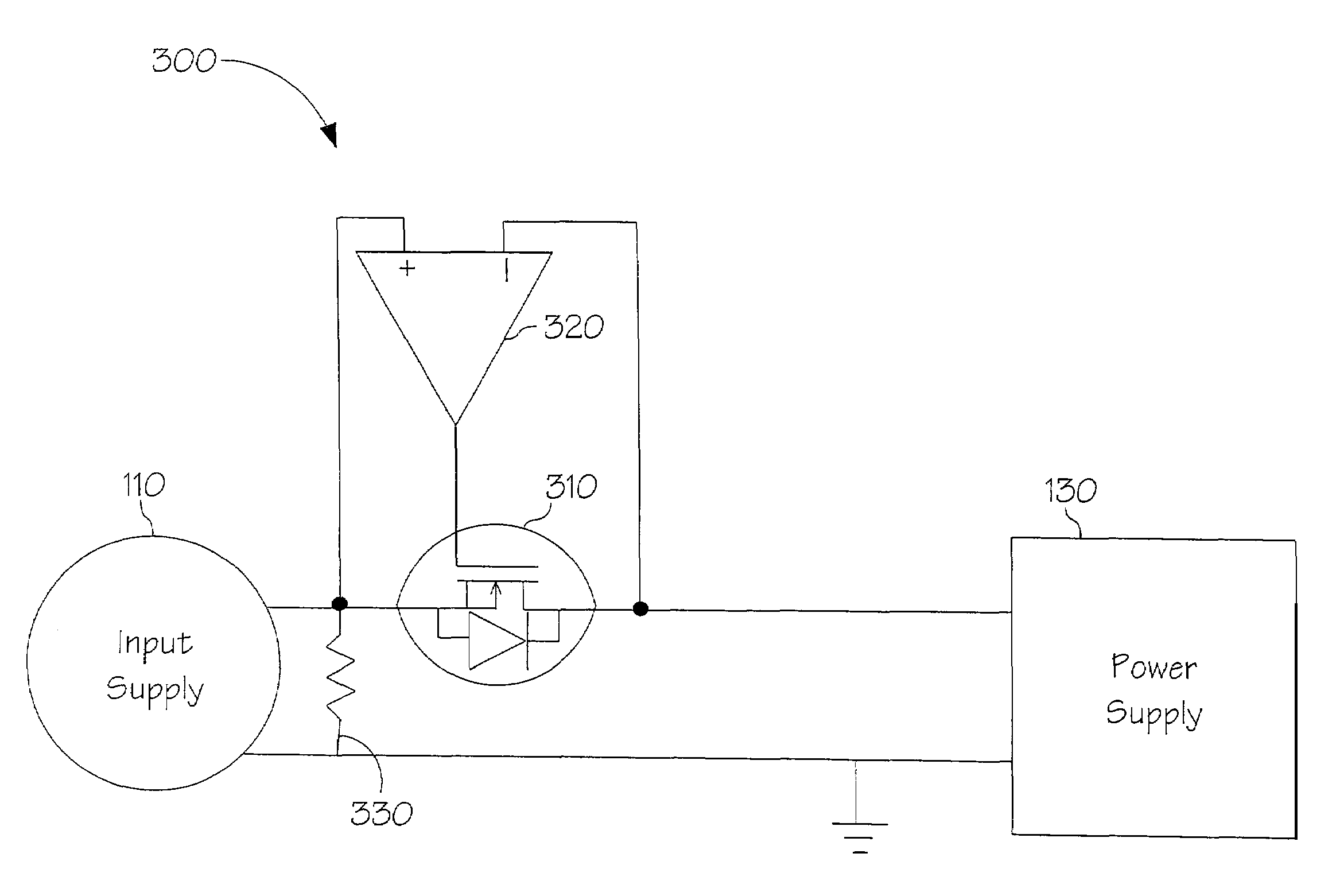
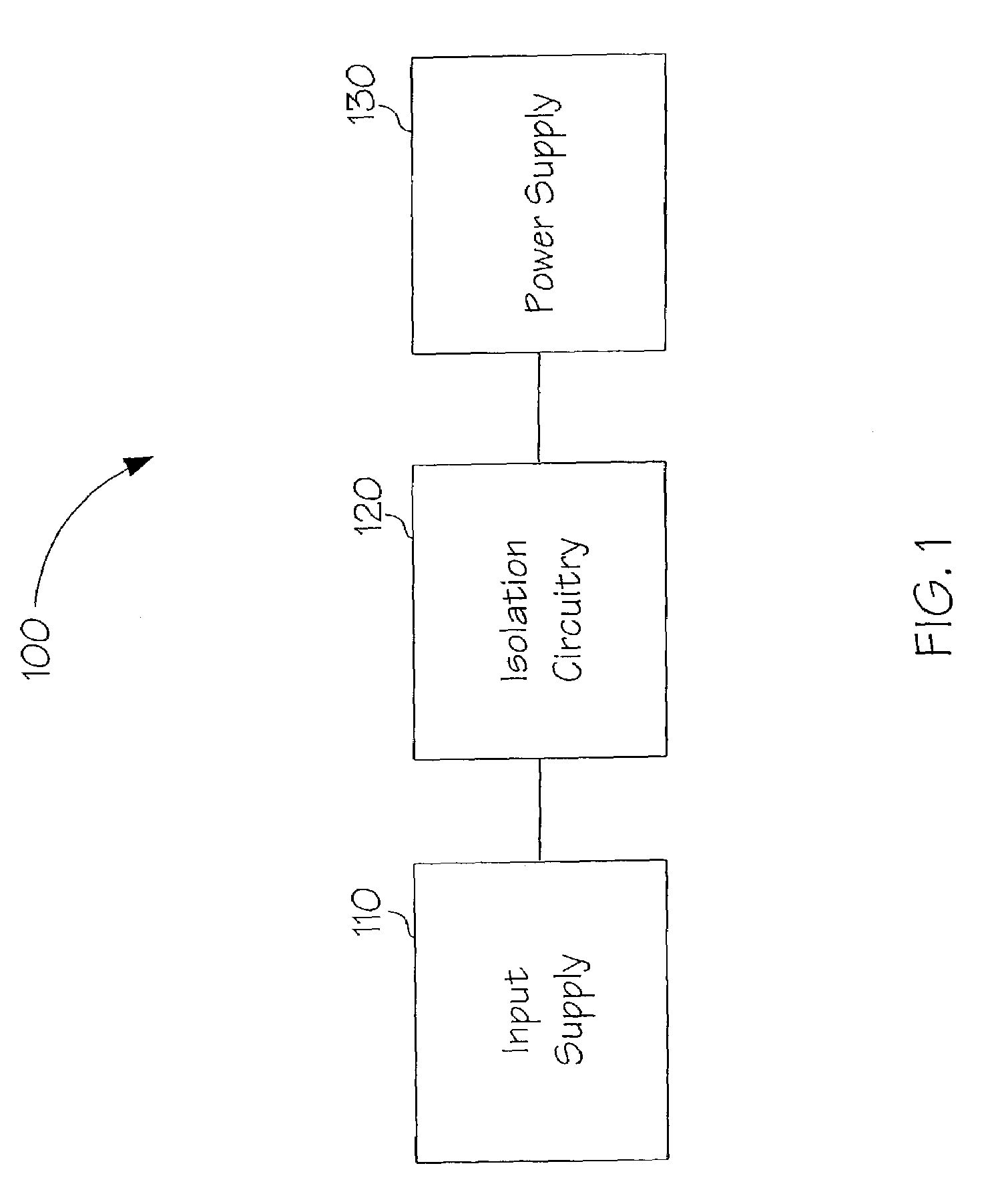
[0013]Referring to FIG. 1, a power supply system 100 in accordance with an embodiment of the present invention is shown. In an embodiment of the invention, power supply system 100 may include an input supply 110, isolation circuitry 120 and a power supply 130. In one embodiment of the invention, input supply 110 may be a direct current (DC) voltage source. Power supply 130 may be a DC / DC conversion power supply capable of receiving an unregulated DC voltage source and providing a regulated voltage source. It should be understood by those with ordinary skill in the art that isolation circuitry may be employed with many types of power delivery systems in order to prevent the reverse flow of current without departing from the scope and spirit of the present invention.

[0014]Specifications for a power supply 130 typically inclu...


PUM


Abstract

The present invention is a method and system for providing improved isolation for power supplies while minimizing power dissipation. A body diode of a MOSFET may be utilized with a comparator circuit. The comparator circuit may detect current flow across the MOSFET and may turn the MOSFET on. This may shunt the diode with a low drain to source resistance limiting power dissipation across the diode to an amount of the drain to source current squared (Ids2) times the drain to source resistance of the MOSFET when on (RDSon). Use of the comparator circuitry may reduce the time delay associated with turning the MOSFET off to prevent a high reverse inrush current within a power supply.

Description

FIELD OF THE INVENTION[0001]The present invention generally relates to the field of power supplies, and more particularly to a method and system for providing isolation for power supplies while minimizing power dissipation for input and output diodes.BACKGROUND OF THE INVENTION[0002]Conventional power supply electric safety specifications require that input terminals of a power supply have no voltage when a power source for the power supply is shut down. In order to meet this requirement, power supply designers typically employ an “OR” diode in series with the input bus to prevent input storage capacitor charge to flow backward to the input terminals of the power supply. This may eliminate fire and electrical shock hazards. Additionally, an “OR” diode may also be utilized in redundant power supply systems at the outputs of parallel connected power supplies to prevent a power supply with a low output voltage from drawing current from a power supply with a higher output voltage or vic...

Claims


Application Information

Patent Timeline
Patent Type & Authority Patents(United States)
IPC IPC(8): H02H7/00
CPCH02J1/108H03K17/063H03K17/76H03K17/6877H03K2017/307H03K17/693
Inventor ZANSKY, ZOLTAN
Owner NETWORK APPLIANCE INC
Why Eureka
Try Eureka