Hall sensor

a sensor and semiconductor technology, applied in the field of semiconductor hall elements and semiconductor hall sensors, can solve the problems of partial cancellation of offset voltage and uneven electric potential distribution, and achieve the effects of reducing chip size, reducing cost, and eliminating offset voltag

Inactive Publication Date: 2017-07-13
ABLIC INC
View PDF1 Cites 2 Cited by
  • Summary
  • Abstract
  • Description
  • Claims
  • Application Information

AI Technical Summary

Benefits of technology

[0032]Through use of the above-mentioned measures, in the Hall sensor including elements serving as the heat sources out of components of the circuit configured to drive the Hall element, even when a temperature distribution is generated in the Hall element due to the influence of the heat generation, the offset voltage can be eliminated by the spinning current.
[0033]Moreover, since a complex circuit is not used and the distance between the heat source and the Hall element does not increase, the offset voltage can be eliminated, the chip size can be reduced and the cost can be suppressed.

Problems solved by technology

Reason for the appearance of the offset voltage is considered to be imbalance of electric potential distribution inside the element due to, for example, mechanical stress applied to the element from the outside thereof or misalignment occurring in a manufacturing process.
However, the offset voltage may not completely be cancelled by this offset cancellation circuit.
However, when this assumption is not satisfied, for example, when R1=R3 is established for one direction but this relationship is not established for the other direction, the difference may not be made zero, and hence the offset may not be cancelled.

Method used


Image

  • Hall sensor
  • Hall sensor
  • Hall sensor

Examples


first embodiment

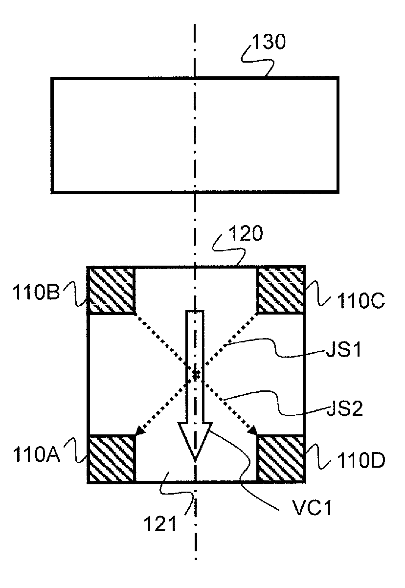
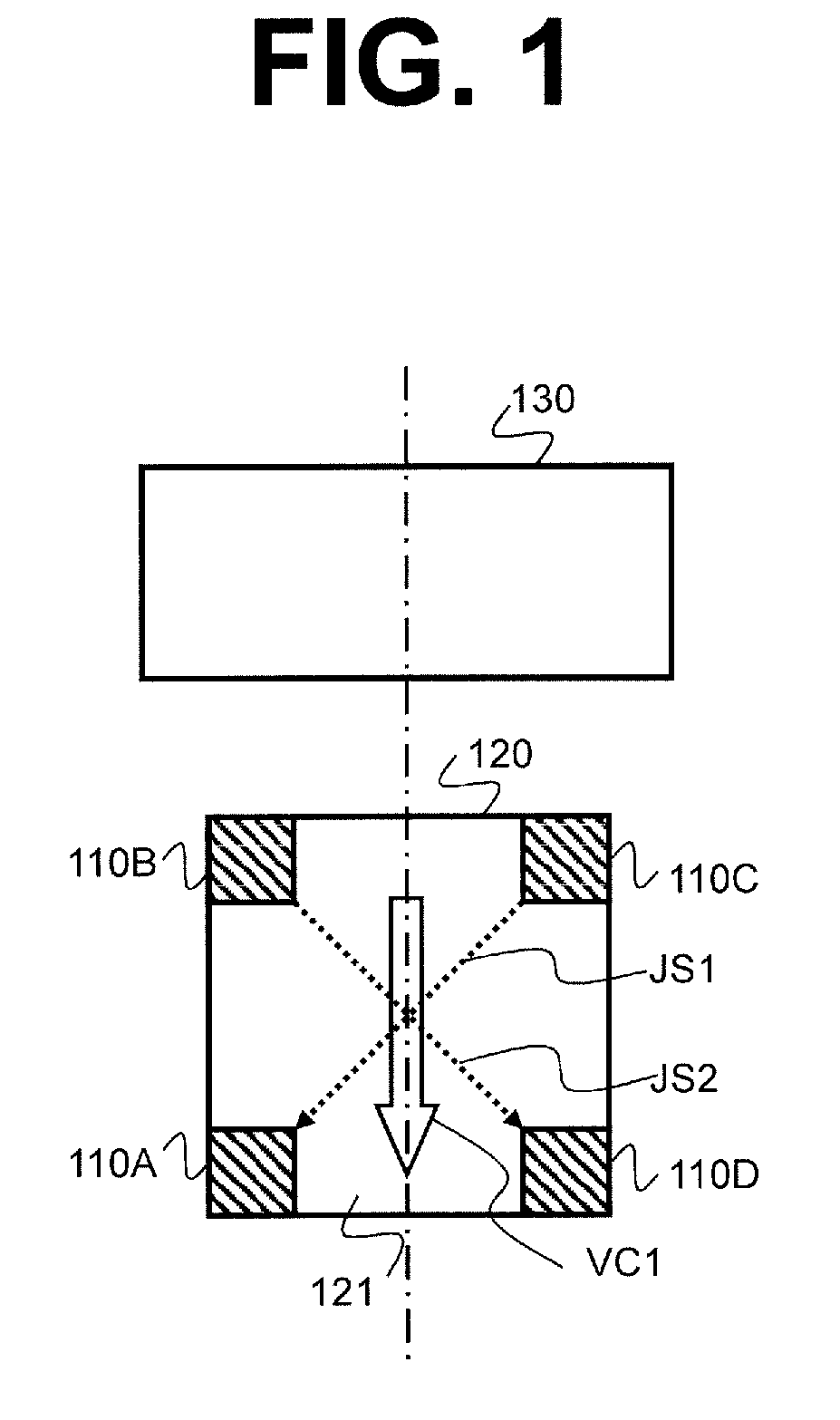
[0043]FIG. 1 is a plan view for illustrating a Hall sensor according to a first embodiment of the present invention. The Hall sensor includes a Hall element configured to sense magnetism and a circuit configured to drive or control the Hall element.

[0044]First, a description is given of a shape of the Hall element. As illustrated in FIG. 1, a Hall element 120 includes, on a semiconductor substrate, a magnetism sensing portion constructed by a square N-type doped region 121 and control current input terminals and Hall voltage output terminals 110A, 110B, 110C, and 110D constructed by N-type highly-doped regions having the same shape, which are arranged at respective vertices of the square magnetism sensing portion. The Hall element 120 is configured as described above, resulting in a symmetrical Hall element.

[0045]A description is now given of a positional relationship between the Hall element and a heat source. A circuit configured to drive the Hall element 120 is arranged on the su...

second embodiment

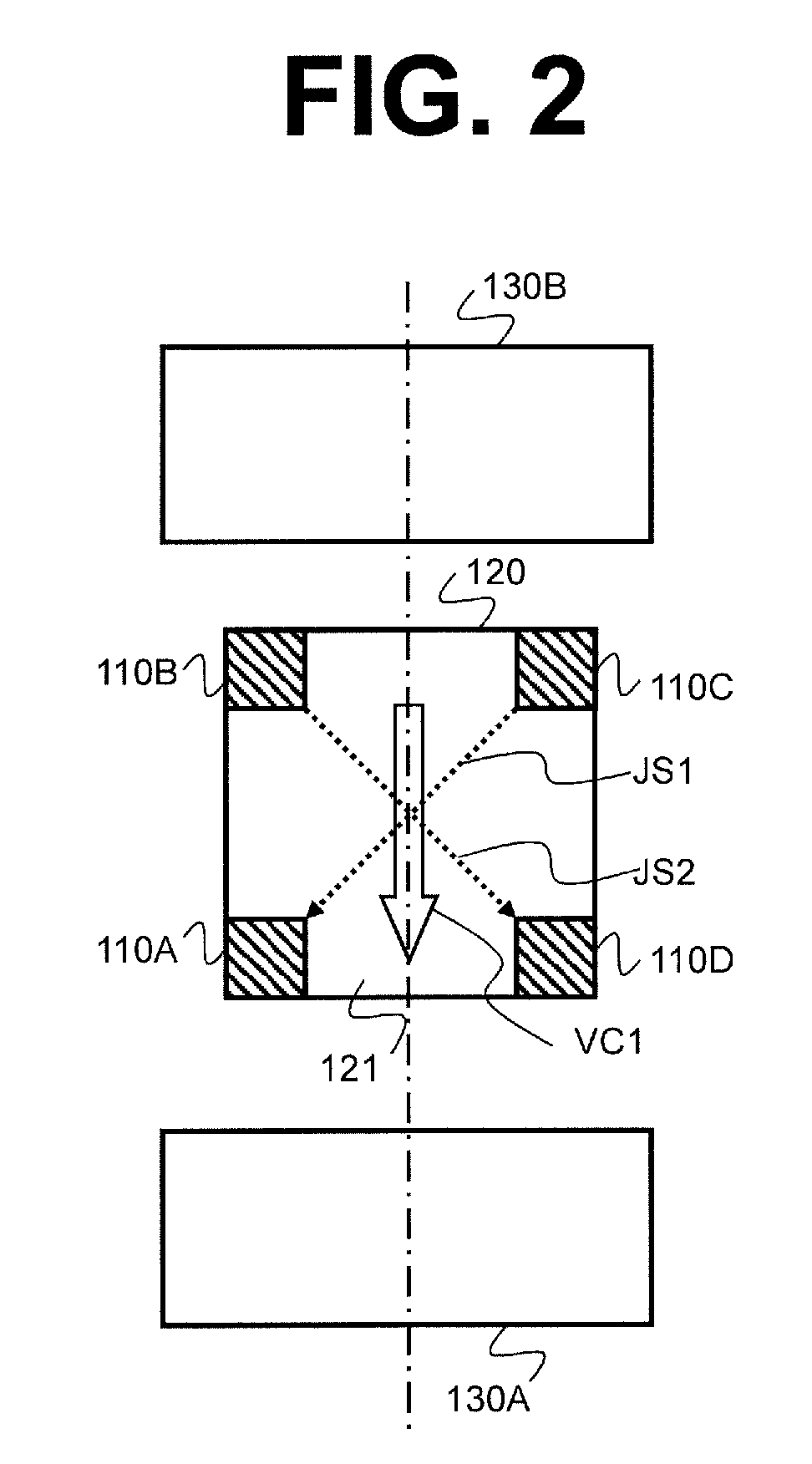
[0057]In the first embodiment, referring to FIG. 1, a description is given of the case where the number of the heat sources is one, but the number of elements that generate heat out of components of the circuit configured to control the Hall element is not limited to one. FIG. 2 is a plan view for illustrating a Hall sensor according to an embodiment of the present invention that includes a plurality of elements (heat sources) 130A and 130B that generate heat out of components of the circuit configured to control the Hall element 120.

[0058]Even in the case where the plurality of heat sources exist, the offset may be eliminated by aligning the centers of the respective heat sources 130A and 130B with an extension line of the vector sum VC1 of the Hall element control currents JS1 and JS2 in the two directions by the spinning current method.

[0059]On this occasion, the center of the heat source means a point or a region having the highest temperature corresponding to a peak of isotherm...

third embodiment

[0061]Further, as illustrated in FIG. 3, when the heat source needs to be arranged in a direction perpendicular to that of FIG. 1 and FIG. 2, the offset may be eliminated by optimizing the directions of the Hall element control currents JS1 and JS2 so as to align the center of the heat source 130 with the extension line of the vector sum VC1 of the Hall element control currents JS1 and JS2.


PUM


Abstract

A Hall sensor includes a Hall element and a heat source element in a circuit configured to drive the semiconductor Hall element, and capable of eliminating an offset voltage without increasing a chip size. In the Hall sensor, a Hall element control current flowing between one pair of terminals out of two pairs and a Hall element control current flowing between another pair of terminals cross each other as vectors, the Hall element has a shape that is line-symmetrical to the straight line along a vector sum of the Hall element control current and the Hall element control current, and the heat source element is arranged so that the center of the heat source is positioned on the straight line along the vector sum of the Hall element control current and the Hall element control current.

Description

RELATED APPLICATIONS[0001]The present application is a continuation of International Application PCT / JP2015 / 074318, with an international filing date of Aug. 28, 2015, which claims priority to Japanese Patent Application No. 2014-202015 filed on Sep. 30, 2014, the entire contents of which are incorporated herein by reference.BACKGROUND OF THE INVENTION[0002]Technical Field[0003]The present invention relates to a semiconductor Hall element and a Hall sensor including a circuit configured to drive the semiconductor Hall element, in particularly, to a Hall sensor capable of eliminating an offset voltage.[0004]Background Art[0005]First, the principle of magnetic detection by a Hall element is described. When a magnetic field is applied perpendicularly to a current flowing through a substance, an electric field (Hall voltage) is generated in a direction perpendicular to both the current and the magnetic field. The principle of the magnetic detection by the Hall element is to acquire an i...

Claims


Application Information

Patent Timeline
Patent Type & Authority Applications(United States)
IPC IPC(8): G01R33/07H01L43/06
CPCH01L43/06G01R33/075H10N52/101G01R33/07H10N52/00
Inventor HIOKA, TAKAAKIHIKICHI, TOMOKI
Owner ABLIC INC
Why Eureka
Try Eureka