Display device and driving method therefor

a technology of a display device and a driving method, which is applied in the direction of static indicating devices, instruments, electroluminescent light sources, etc., can solve the problems of difficult to achieve size increase and definition improvement, difficult to achieve definition improvement, etc., to suppress display unevenness or vertical stripes, low resolution image, and low driving frequency

Active Publication Date: 2017-07-13
SHARP KK
View PDF2 Cites 17 Cited by
  • Summary
  • Abstract
  • Description
  • Claims
  • Application Information

AI Technical Summary

Benefits of technology

[0091]According to the first aspect of the present invention, intervals of electro-optical elements which go into a light-emitting state in each unit frame when in the low resolution mode is equalized regarding a direction in which the scanning signal lines extend. Accordingly, occurrence of display unevenness (color unevenness) or vertical stripes is suppressed, and an image with which viewers do not feel uncomfortable is displayed.
[0092]According to the second aspect of the present invention, when a low resolution image is displayed, j pixel circuits are defined as one group, and electro-optical elements having respective light-emitting colors different from one another are brought into a light-emitting state in j pixel circuits included in each group. Hence, a color image with a resolution not more than 1/j of a resolution in the time-division driving can be displayed by one vertical scanning. In this way, in a display device that adopts the time-division driving, it is possible to display a low resolution image while lowering the driving frequency. Accordingly, by switching, depending on the magnitude of demand regarding a definition of a display image, for example, the display mode between a high resolution mode, in which a high resolution image is displayed by the time-division driving, and a low resolution mode, in which a low resolution image is displayed by a driving method whose driving frequency is lower than that of the time-division driving, power consumption can be reduced compared to that in a case where image display is always performed by the time-division driving. Moreover, when in the low resolution mode, momentary luminances of the electro-optical elements do not need to be increased compared to those in a case where the time-division driving is performed. Thus, shortening of the lifetime of the electro-optical el

Problems solved by technology

An organic EL display device adopting the passive matrix system is simple in structure, but is difficult to achieve size increase and definition improvement.
Acc

Method used


Image

  • Display device and driving method therefor
  • Display device and driving method therefor
  • Display device and driving method therefor

Examples


first embodiment

1. First Embodiment

[0164]

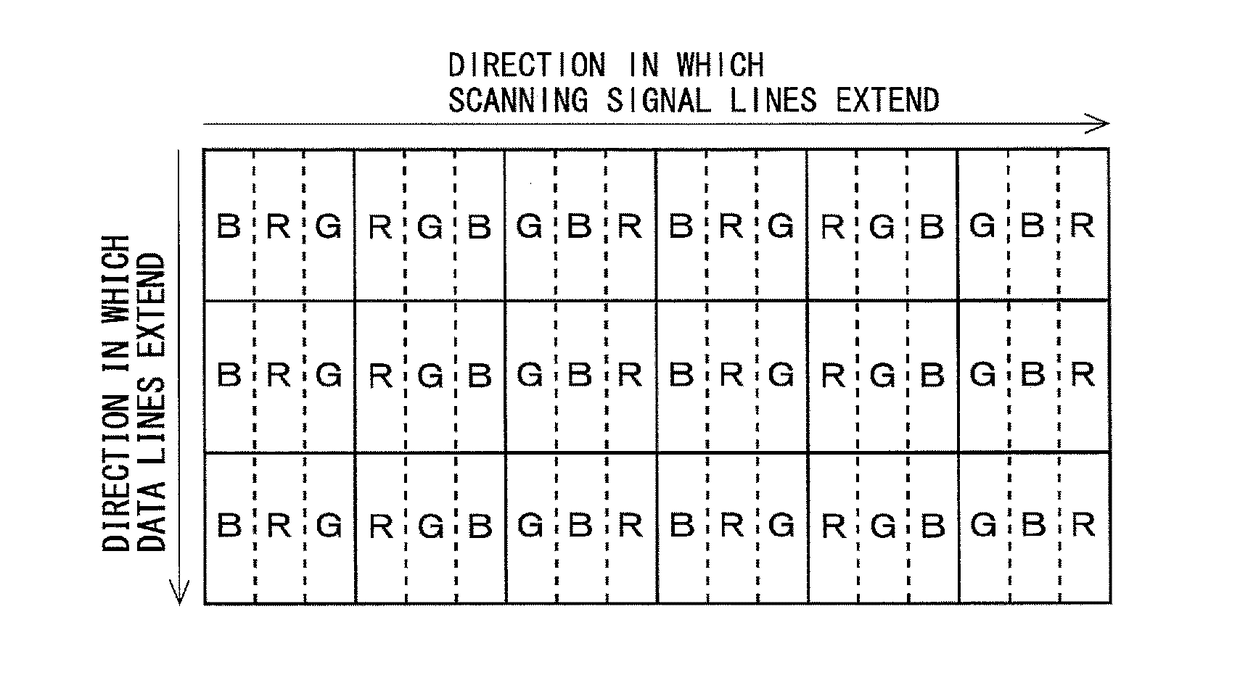
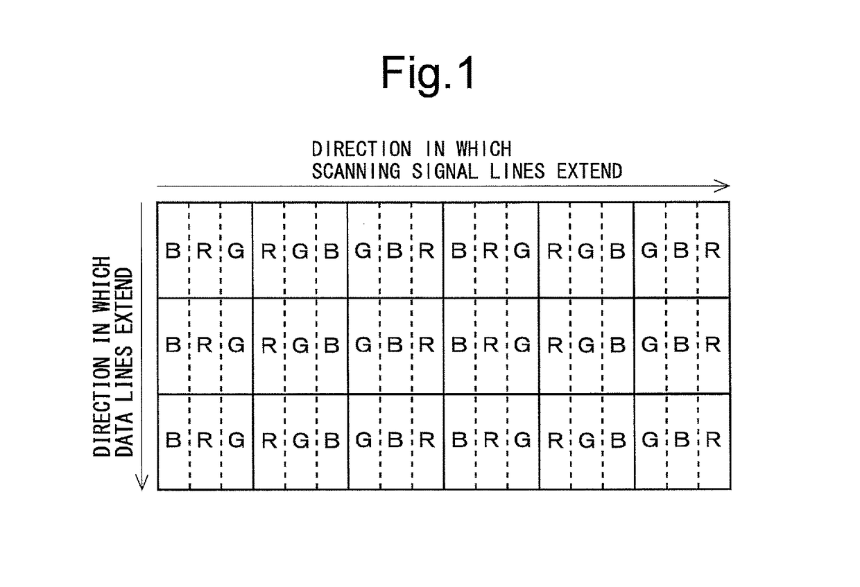
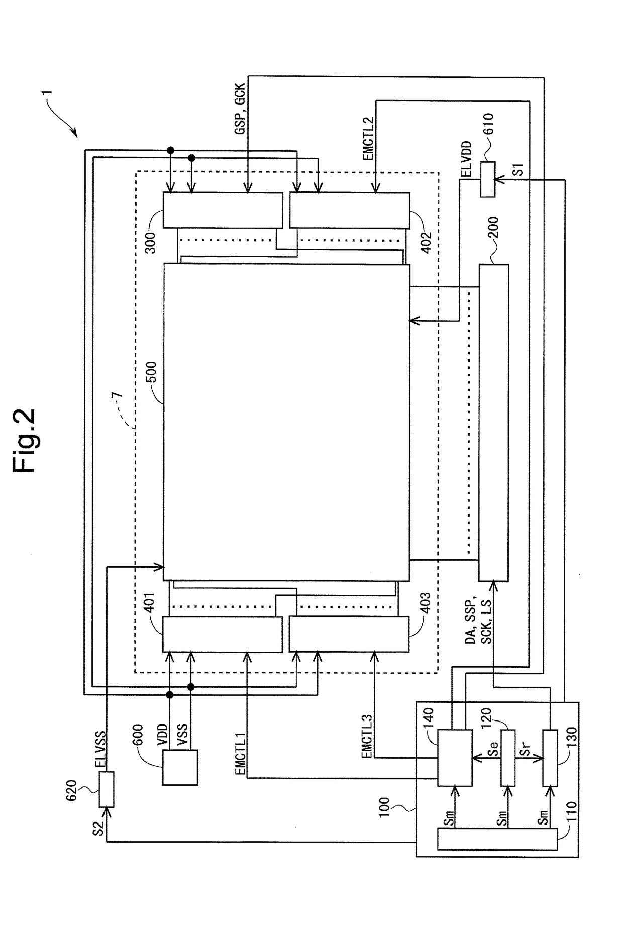
[0165]FIG. 2 is a block diagram showing an overall configuration of an active matrix-type organic EL display device 1 according to a first embodiment of the present invention. The organic EL display device 1 includes a display control circuit 100, a source driver (a data line drive circuit) 200, a gate driver (a scanning signal line drive circuit) 300, first to third emission drivers (first to third light-emission control line drive circuits) 401 to 403, and a display unit 500. The first to third emission drivers 401 to 403 are hereinafter also collectively and simply referred to as “emission driver”. The emission driver is a drive circuit for wiring lines (emission lines which will be described later) for controlling the light emission of organic EL elements provided in the display unit 500. Note that in the present embodiment the gate driver 300 and the first to third emission drivers 401 to 403 are formed in an organic EL panel 7 including the display uni...

second embodiment

2. Second Embodiment

[0242]

[0243]A second embodiment of the present invention will be described. In recent years, in order to realize a reduction in power consumption in a display device, developments have been made in a driving method involving “providing a pause period during which a write operation of image data pauses by bringing all scanning signal lines into a non-scanning state, between a refresh period (a writing period) and a refresh period (a writing period)”. Such a driving is called, for example, “pause driving”. In a display device adopting the pause driving, since it can bring the operation of the peripheral drivers to a halt in the pause period, power consumption can be reduced. Also in the organic EL display device, the pause driving like this is being adopted. Therefore, an organic EL display device adopting the pause driving will be described as a second embodiment of the present invention. Note that an overall configuration (see FIG. 2), an arrangement of pixels (s...


PUM


Abstract

When a display mode is a high-resolution mode, image display is performed by time division driving. When the display mode is a low-resolution mode, image display is performed by defining j pixel circuits arranged continuously in a direction in which scanning signal lines extend as one group, bringing only one organic EL element into a light-emitting state in each of the pixel circuits in a frame period, and bringing organic EL elements having respective light emission colors different from one another into a light-emitting state in the j pixel circuits included in each group in the frame period. Pixel circuits in a display unit are configured such that the intervals of organic EL elements which go into a light-emitting state in the frame period when in the low-resolution mode are equalized regarding a direction in which the scanning signal lines extend.

Description

TECHNICAL FIELD[0001]The present invention relates to a display device and more particularly to a display device including self light-emitting type display elements which are driven by a current, such as an organic EL display device, and a method for driving the display device.BACKGROUND ART[0002]Conventionally, as display elements included in a display device, there are an electro-optical element whose luminance is controlled by a voltage applied thereto, and an electro-optical element whose luminance is controlled by a current flowing therethrough. A representative example of the electro-optical element whose luminance is controlled by a voltage applied thereto includes a liquid crystal display element. On the other hand, a representative example of the electro-optical element whose luminance is controlled by a current flowing therethrough includes an organic EL (Electro Luminescence) element. The organic EL element is also called an OLED (Organic Light-Emitting Diode). An organic...

Claims


Application Information

Patent Timeline
IPC IPC(8): G09G3/3258H01L51/50H01L27/32H01L27/12G09G3/3266G09G3/34H05B44/00
CPCG09G3/3258G09G3/3266G09G3/3413H01L27/3276G09G2320/0242H01L27/3211H01L51/5012G09G2310/08G09G2340/0407H01L27/1225G09G3/3233G09G2300/0814G09G2300/0842G09G2300/0861H10K59/351H10K59/35H10K50/11H10K59/131
Inventor NOGUCHI, NOBORUOHARA, MASANORIKISHI, NORITAKA
Owner SHARP KK
Why Eureka
Try Eureka