Display device, semiconductor device, and driving method thereof

a technology of semiconductor devices and drive methods, applied in semiconductor devices, digital storage, instruments, etc., can solve the problems of narrow drive frequency range difficult to lower the drive frequency of semiconductor devices such as gate driver circuits, and loss of electric charge stored in the gate of pull-up transistors as time passes, so as to reduce the drive frequency of semiconductor devices and improve the operation of semiconductor devices. , the effect of widening the drive frequency rang

Active Publication Date: 2013-12-03
SEMICON ENERGY LAB CO LTD
View PDF170 Cites 12 Cited by
  • Summary
  • Abstract
  • Description
  • Claims
  • Application Information

AI Technical Summary

Benefits of technology

[0006]In view of the problems, an object of one embodiment of the present invention is to improve operation of a semiconductor device including a transistor (a pull-up transistor) that controls the timing of when a predetermined voltage is outputted to a circuit located at the subsequent stage. An object of one embodiment of the present invention is to improve the drive capability of a semiconductor device including a transistor (a pull-up transistor) that controls the timing of when a predetermined voltage is outputted to a circuit located at the subsequent stage.
[0007]One embodiment of the present invention is a semiconductor device including a first transistor, and a second transistor electrically connected to a gate of the first transistor. A first terminal of the first transistor is electrically connected to a first line. A second terminal of the first transistor is electrically connected to a second line. The gate of the first transistor is electrically connected to a first terminal or a second terminal of the second transistor. In the semiconductor device, the first transistor and the second transistor can have an oxide semiconductor at least in their channel regions and have a low off-state current. Alternatively, at least the second transistor can have an oxide semiconductor at least in its channel region and have a low off-state current. Specifically, the first transistor or the second transistor can have an off-state current of 1 aA / μm or less per 1 μm of channel width at room temperature (20° C. in this case). One or more of the second transistors can be provided in the semiconductor device. It is preferable that when a plurality of the second transistors is provided, all these transistors have an oxide semiconductor at least in their channel regions and have a low off-state current. In the semiconductor device, the second line can be electrically connected to a circuit located at the subsequent stage. Thus, the first transistor can serve as a transistor (a pull-up transistor) that controls the timing of when a predetermined voltage is outputted to the circuit located at the subsequent stage.
[0014]One embodiment of the present invention is a semiconductor device including a transistor (a pull-up transistor) that controls the timing of when a high voltage is outputted to a circuit located at the subsequent stage. In this semiconductor device, charge stored in a gate of the pull-up transistor is held for a long period of time. Therefore, it is possible to reduce the drive frequency of the semiconductor device and to widen the range of the drive frequency at which the semiconductor device can operate. Thus, the operation of the semiconductor device can be improved. Alternatively, the drive capability of the semiconductor device can be improved.

Problems solved by technology

In conventional techniques, however, even when all the transistors that are connected to a gate of a pull up transistor are turned off, electrical charge stored in the gate of the pull up transistor is lost as time passes because of the off-state current of the transistor.
It is therefore difficult to lower the drive frequency of a semiconductor device such as a gate driver circuit.
Further, the range of the drive frequency at which the semiconductor device can operate is narrow.
Consequently, there is a limit to improvement in the drive capability of the semiconductor device.

Method used


Image

  • Display device, semiconductor device, and driving method thereof
  • Display device, semiconductor device, and driving method thereof
  • Display device, semiconductor device, and driving method thereof

Examples


embodiment 1

[0031]In this embodiment, a circuit in a display device that is one embodiment of the present invention will be described.

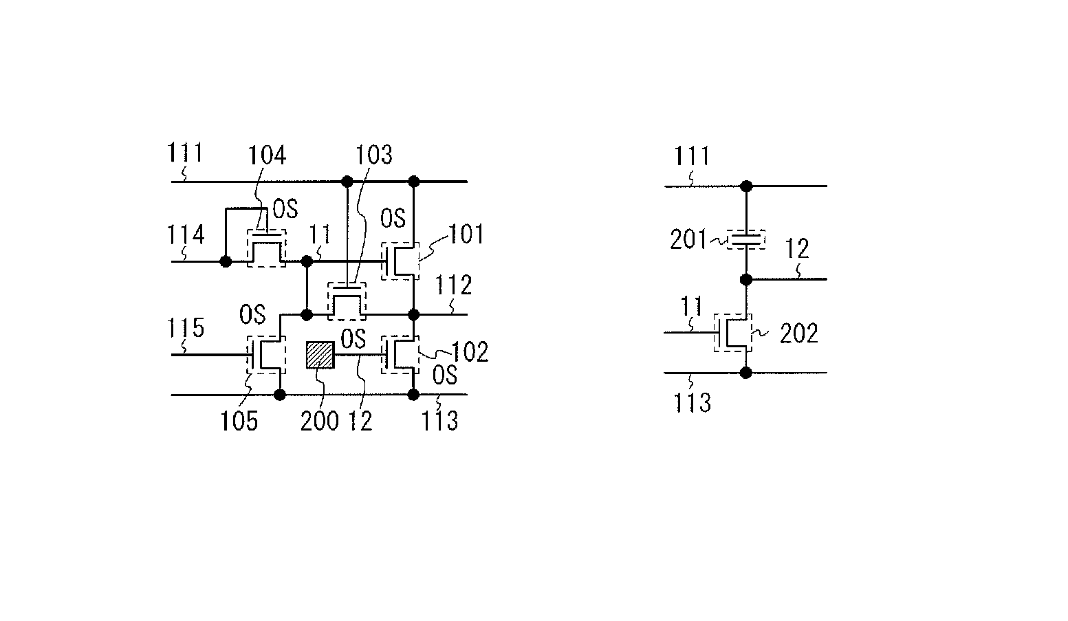
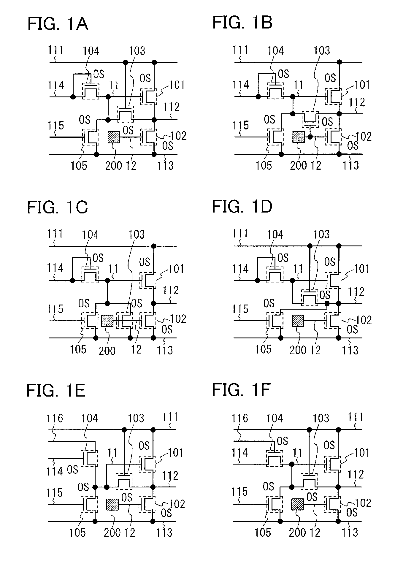
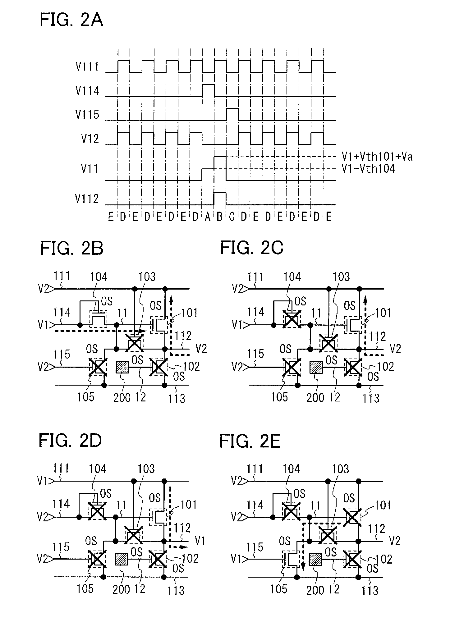
[0032]FIG. 1A shows an example of the configuration of a circuit including a transistor 101, a transistor 102, a transistor 103, a transistor 104, a transistor 105, and a circuit 200. The transistors included in the circuit shown in FIG. 1A are n-channel transistors. An n-channel transistor is turned on when a potential difference between a gate and a source is higher than the threshold voltage.

[0033]Note that the transistors included in the circuit shown in FIG. 1A can each have a semiconductor layer of an oxide semiconductor that is intrinsic (i-type) or substantially intrinsic, has an adequately lowered hydrogen concentration which makes the oxide semiconductor highly purified, and has an adequately low carrier concentration. This leads to improvement in the subthreshold swing of the transistor, a reduction in the off-state current of the transistor, improveme...

embodiment 2

[0081]In this embodiment, a shift register circuit in a display device which is one embodiment of the present invention will be described. A shift register circuit of this embodiment can include any of the circuits of Embodiment 1. Further, the shift register circuit of this embodiment can be used as a driver circuit of a display device, such as a gate driver circuit and / or a source driver circuit.

[0082]FIG. 8 shows an example of the configuration of a shift register circuit that includes N pieces of circuits 301 (circuits 301_1 to 301_N). Any of the circuits described in Embodiment 1 can be used as the circuit 301. FIG. 8 shows an example of the case where the circuit shown in FIG. 1A is used as the circuit 301.

[0083]Connections in the shift register circuit shown in FIG. 8 will be described. Connections in a circuit 301—i (i is included in 2 to N−1) will be described as an example. The circuit 301—i is connected to a line 311—i, a line 311_ / i−1, a line 311—i+1, either a line 312 o...

embodiment 3

[0092]In this embodiment, an example of a transistor included in the circuit of Embodiment 1 or 2 will be described. Specifically, examples of the structure of a transistor whose channel region is formed using an oxide semiconductor and fabrication steps thereof will be described.

[0093]As the oxide semiconductor, the following oxides can be used: an In—Sn—Ga—Zn—O-based oxide semiconductor that is an oxide of four metal elements; an In—Ga—Zn—O-based oxide semiconductor, an In—Sn—Zn—O-based oxide semiconductor, an In—Al—Zn—O-based oxide semiconductor, a Sn—Ga—Zn—O-based oxide semiconductor, an Al—Ga—Zn—O-based oxide semiconductor, or a Sn—Al—Zn—O-based oxide semiconductor that is an oxide of three metal elements; an In—Zn—O-based oxide semiconductor, a Sn—Zn—O-based oxide semiconductor, an Al—Zn—O-based oxide semiconductor, a Zn—Mg—O-based oxide semiconductor, a Sn—Mg—O-based oxide semiconductor, or an In—Mg—O-based oxide semiconductor that is an oxide of two metal elements; an In—O-b...


PUM


Abstract

An object is to provide a semiconductor device with improved operation. The semiconductor device includes a first transistor, and a second transistor electrically connected to a gate of the first transistor. A first terminal of the first transistor is electrically connected to a first line. A second terminal of the first transistor is electrically connected to a second line. The gate of the first transistor is electrically connected to a first terminal or a second terminal of the second transistor.

Description

TECHNICAL FIELD[0001]One embodiment of the present invention relates to display devices. For example, one embodiment of the present invention relates to liquid crystal display devices. One of the technical fields relates to a display device in which an image is displayed when a pixel is selected by a gate signal line and a source signal line. Further, one of the technical fields relates to an electronic appliance with a display device and a semiconductor device such as a driver circuit used in a display device.BACKGROUND ART[0002]Gate driver circuits including amorphous silicon transistors (also referred to as a-Si TFTs) have been developed (see Patent Documents 1 and 2, for example). Such a gate driver includes a transistor for controlling the timing of outputting a high voltage to a gate line (such a transistor is also referred to as a pull up transistor). The pull up transistor has a source and a drain one of which is connected to a clock line and the other of which is connected ...

Claims


Application Information

Patent Timeline
Patent Type & Authority Patents(United States)
IPC IPC(8): G11C19/00
CPCG11C19/28H01L27/1225G09G3/3677G09G2310/0286G09G3/3674G09G3/20G11C19/287H01L27/124H01L29/7869
Inventor UMEZAKI, ATSUSHIKIMURA, HAJIME
Owner SEMICON ENERGY LAB CO LTD
Why Eureka
Try Eureka