Pulse signal output circuit and shift register

a shift register and output circuit technology, applied in static indicating devices, instruments, optics, etc., can solve the problems of difficult to lower the drive frequency of a semiconductor device such as a gate driver circuit, limit the reduction in the circuit size of a semiconductor device, and lose electrical charges accumulated in the gate of the pull up transistor, etc., to achieve the reduction of the number of transistors serving as pull down transistors, the effect of suppressing hot carrier degradation of the pull down transistor and small circuit size of a semiconductor

Active Publication Date: 2013-12-10
SEMICON ENERGY LAB CO LTD
View PDF133 Cites 11 Cited by
  • Summary
  • Abstract
  • Description
  • Claims
  • Application Information

AI Technical Summary

Benefits of technology

[0009]Note that the band gap of the oxide semiconductor is 2.0 eV or more, preferably 2.5 eV or more, more preferably 3.0 eV or more. Thus, in the transistor whose channel region includes the oxide semiconductor, impact ionization and avalanche breakdown do not easily occur. That is, carriers (electrons) in the oxide semiconductor are not easily accelerated. Therefore, in the transistor whose channel region includes the oxide semiconductor, fluctuations in the threshold voltage of the transistor due to injection of carriers (electrons) into a gate insulating layer (so-called hot carrier degradation) can be suppressed.
[0019]In one embodiment of the present invention, a transistor whose channel region includes an oxide semiconductor is used as a pull down transistor. Thus, hot carrier degradation in the pull down transistor can be suppressed. Therefore, the number of transistors serving as pull down transistors can be reduced. Accordingly, the size of a circuit for controlling the on-off of a pull down transistor can be made small. Consequently, the circuit size of a semiconductor device including the pull down transistor can be made small.
[0020]Further, in one embodiment of the present invention, a gate of a pull up transistor is made to be in a floating state by switching of the on-off of a transistor whose channel region includes an oxide semiconductor. Thus, electrical charges accumulated in the gate of the pull up transistor can be held for a long period of time. Therefore, the drive frequency of a semiconductor device including the pull up transistor can be lowered. Further, the range of drive frequency at which the semiconductor device can operate can be broadened. Accordingly, the drive capability of the semiconductor device can be improved.

Problems solved by technology

Thus, there is a limit to the decrease in the circuit size of a semiconductor device.
In addition, even when all the transistors that are connected to a gate of the pull up transistor are turned off, electrical charges accumulated in the gate of the pull up transistor are lost due to the off-state current of the transistor as time passes.
Therefore, it is difficult to lower the drive frequency of a semiconductor device such as a gate driver circuit.
Accordingly, there is a limit to improvement in the drive capability of the semiconductor device.
Thus, in the transistor whose channel region includes the oxide semiconductor, impact ionization and avalanche breakdown do not easily occur.
That is, carriers (electrons) in the oxide semiconductor are not easily accelerated.

Method used


Image

  • Pulse signal output circuit and shift register
  • Pulse signal output circuit and shift register
  • Pulse signal output circuit and shift register

Examples


embodiment 1

[0039]In this embodiment, a circuit in a display device which is one embodiment of the present invention is described.

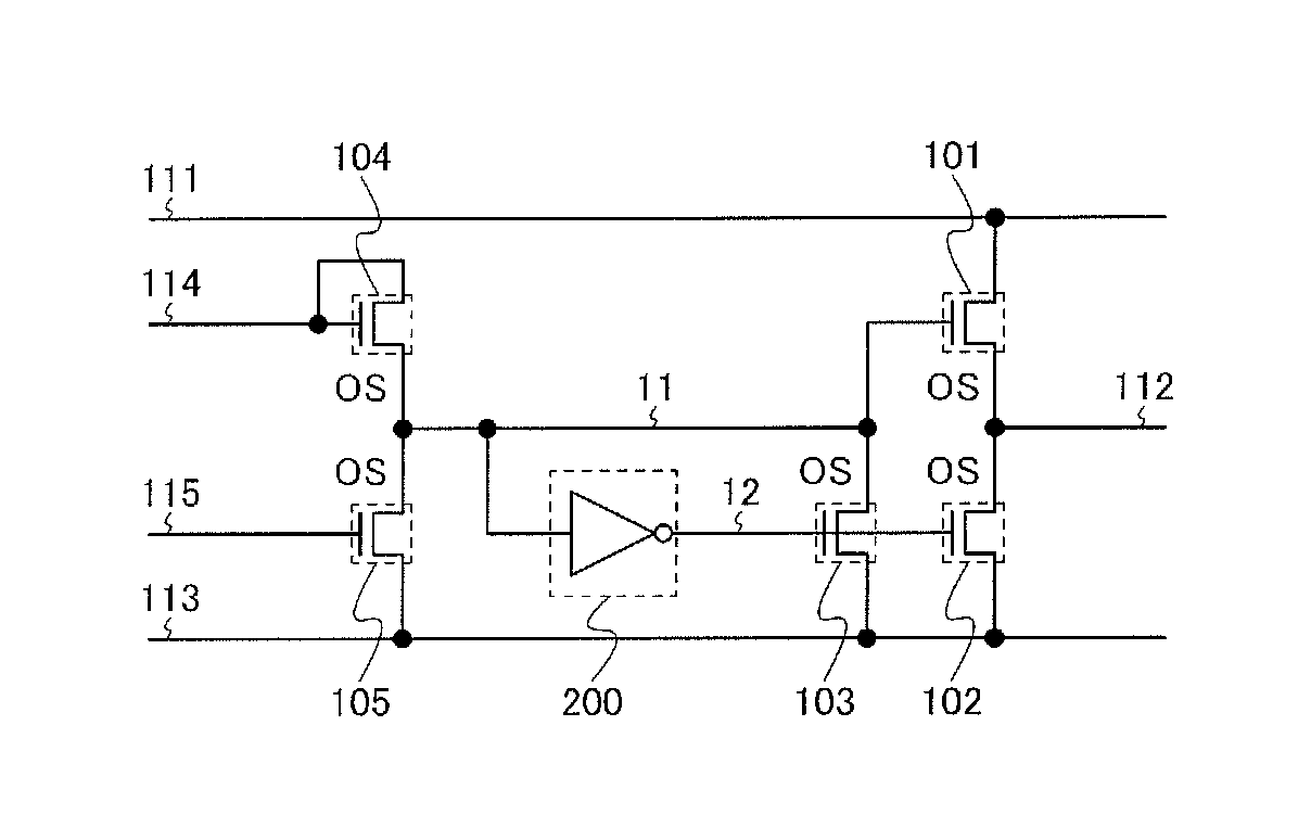
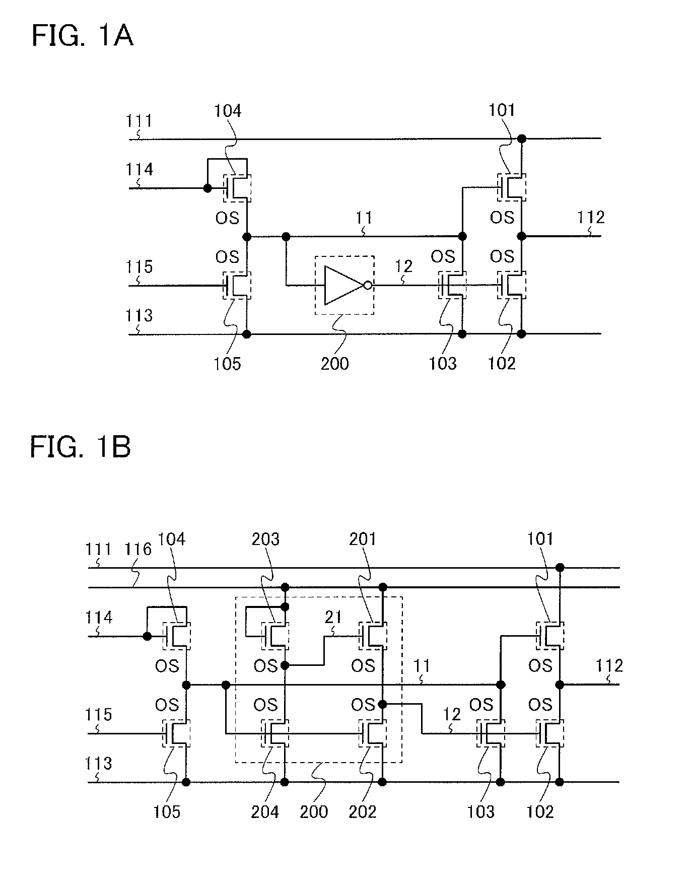
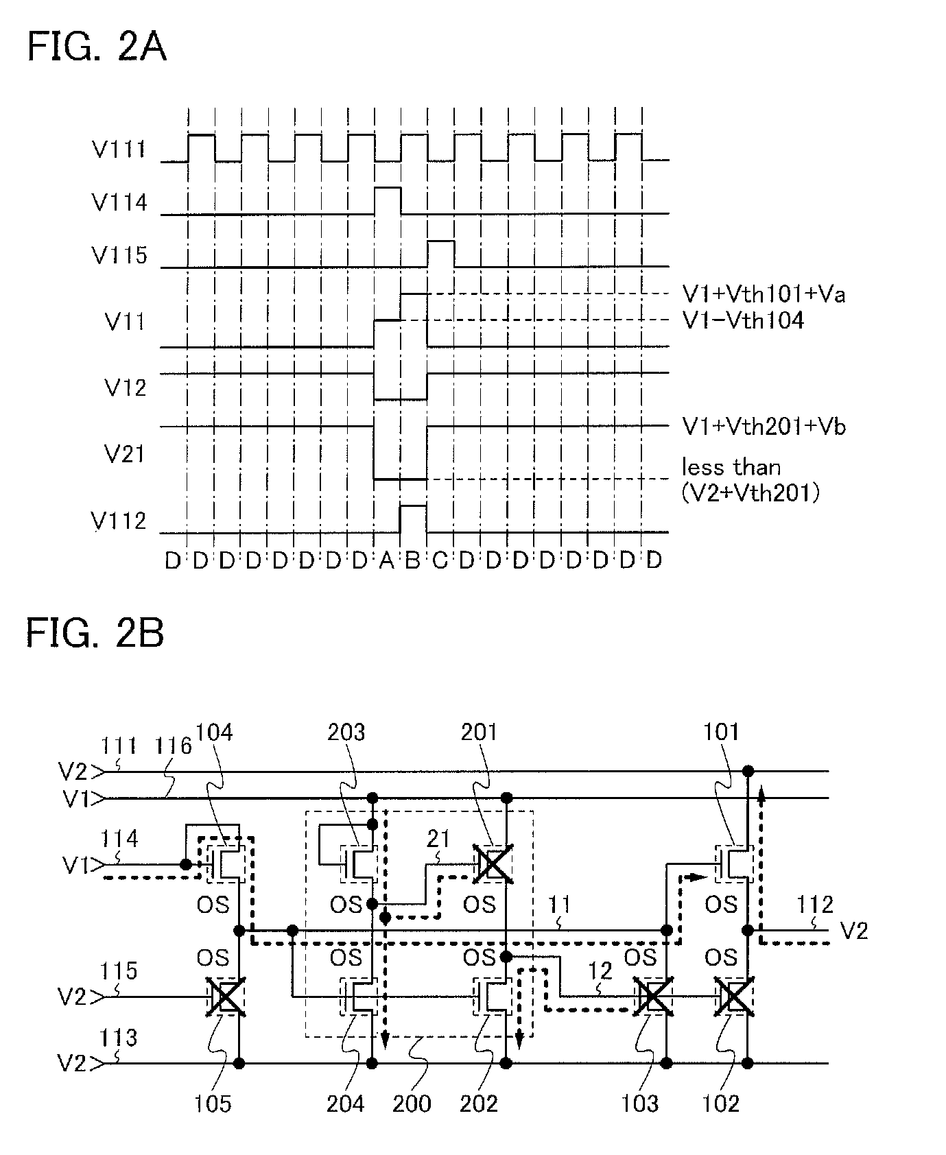
[0040]FIG. 1A illustrates a structure example of a circuit which includes a transistor 101, a transistor 102, a transistor 103, a transistor 104, a transistor 105, and a circuit 200. The transistors included in the circuit illustrated in FIG. 1A are n-channel transistors. An n-channel transistor is turned on when a potential difference between a gate and a source is higher than the threshold voltage.

[0041]Note that an oxide semiconductor may be used for a semiconductor layer of the transistor included in the circuit illustrated in FIG. 1A. It is preferable that the oxide semiconductor be an intrinsic (i-type) or substantially intrinsic oxide semiconductor which is obtained by sufficiently lowering a hydrogen concentration to be highly purified and has sufficiently low carrier density. With the oxide semiconductor, the subthreshold swing of the transistor can be decre...

embodiment 2

[0080]In this embodiment, a shift register circuit in a display device which is one embodiment of the present invention is described. A shift register circuit in this embodiment can include any of the circuits described in Embodiment 1. Further, the shift register circuit in this embodiment can be used as a driver circuit of a display device, such as a gate driver circuit and / or a source driver circuit.

[0081]FIG. 11 illustrates a structure example of a shift register circuit which includes N (N is a natural number) pieces of circuits 301 (circuits 301_1 to 301_N). Any of the circuits described in Embodiment 1 can be used as the circuit 301. FIG. 11 illustrates an example in which the circuit illustrated in FIG. 1A is used as the circuit 301.

[0082]Connection relations in the shift register circuit illustrated in FIG. 11 are described. The connection relation in a circuit 301—i (i is a natural number that is 2 or more and less than N−1) is described as an example. The circuit 301—i is...

embodiment 3

[0088]In this embodiment, an example of a transistor included in the circuit described in Embodiment 1 or 2 is described. Specifically, examples of the structure of a transistor whose channel region includes an oxide semiconductor and manufacturing steps thereof are described.

[0089]As the oxide semiconductor, the following oxides can be used: an In—Sn—Ga—Zn—O-based oxide semiconductor that is an oxide of four metal elements; an In—Ga—Zn—O-based oxide semiconductor, an In—Sn—Zn—O-based oxide semiconductor, an In—Al—Zn—O-based oxide semiconductor, a Sn—Ga—Zn—O-based oxide semiconductor, an Al—Ga—Zn—O-based oxide semiconductor, or a Sn—Al—Zn—O-based oxide semiconductor that is an oxide of three metal elements; an In—Zn—O-based oxide semiconductor, a Sn—Zn—O-based oxide semiconductor, an Al—Zn—O-based oxide semiconductor, a Zn—Mg—O-based oxide semiconductor, a Sn—Mg—O-based oxide semiconductor, or an In—Mg—CD-based oxide semiconductor that is an oxide of two metal elements; an In—O-base...


PUM


Abstract

A transistor whose channel region includes an oxide semiconductor is used as a pull down transistor. The band gap of the oxide semiconductor is 2.0 eV or more, preferably 2.5 eV or more, more preferably 3.0 eV or more. Thus, hot carrier degradation in the transistor can be suppressed. Accordingly, the circuit size of the semiconductor device including the pull down transistor can be made small. Further, a gate of a pull up transistor is made to be in a floating state by switching of on / off of the transistor whose channel region includes an oxide semiconductor. Note that when the oxide semiconductor is highly purified, the off-state current of the transistor can be 1 aA / μm (1×10⁻¹⁸ A / μm) or less. Therefore, the drive capability of the semiconductor device can be improved.

Description

TECHNICAL FIELD[0001]One embodiment of the present invention relates to display devices. For example, one embodiment of the present invention relates to liquid crystal display devices. One of the technical fields relates to display devices in which images are displayed when pixels are selected by gate signal lines and source signal lines. Further, one of the technical fields relates to semiconductor devices such as driver circuits used in display devices and electronic devices including display devices.BACKGROUND ART[0002]Gate driver circuits including amorphous silicon transistors (also referred to as a-Si TFTs) have been developed. Such a gate driver circuit has a problem of malfunctions due to a shift in the threshold voltage of a transistor for keeping the potential of a gate line low (at an L level) (such a transistor is also referred to as a pull down transistor). In order to solve this problem, a gate driver circuit in which a pull down transistor is repeatedly turned on and ...

Claims


Application Information

Patent Timeline
Patent Type & Authority Patents(United States)
IPC IPC(8): G09G5/00
CPCG09G3/3677G11C19/28H01L27/088G09G2310/0286G02F1/13306G02F1/136286G09G3/3648G09G2310/0289G09G2310/08G11C19/287H01L27/1225H01L27/124H01L29/42356H01L29/7869
Inventor UMEZAKI, ATSUSHIKIMURA, HAJIME
Owner SEMICON ENERGY LAB CO LTD
Why Eureka
Try Eureka