Method for Optical and Electrical Signal Processing of a Multi-Heterodyne Signal Generated by a Multi-Mode Semi-Conductor Laser and Detection Device Utilizing that Method

Active Publication Date: 2017-07-13
ETH ZZURICH
View PDF13 Cites 15 Cited by
  • Summary
  • Abstract
  • Description
  • Claims
  • Application Information

AI Technical Summary

Benefits of technology

[0017]Furthermore, the invention allows resolving unambiguously the mirroring problem of a multi-heterodyne spectrometer. When acquiring a multi-heterodyne measurement, the acquired spectrum can be mirrored in the down-mixed RF-frequency domain. This is very problematic, when running fitting software on the acquired data, for example to determine the concentration of species present in the absorbing sample. The fitting software must be run twice, once on the original data, once on the mirrored data. This slows clown the acquisition software and adds a possible error source of the result. The present method, device and system allows to measure and to know the minoring condition of the multi-heterodyne system before the data analysis is performed, reducing the complexity of the system and enhancing

Problems solved by technology

In a typical multi-heterodyne spectrometer setup, this mode spacing determines the spectral sampling of the investigated sample and therefore ultimately limit the spectral resolution of the setup.
Depending on the application, this limits severely the performance of the system.
Depending on the investiga

Method used


Image

  • Method for Optical and Electrical Signal Processing of a Multi-Heterodyne Signal Generated by a Multi-Mode Semi-Conductor Laser and Detection Device Utilizing that Method
  • Method for Optical and Electrical Signal Processing of a Multi-Heterodyne Signal Generated by a Multi-Mode Semi-Conductor Laser and Detection Device Utilizing that Method
  • Method for Optical and Electrical Signal Processing of a Multi-Heterodyne Signal Generated by a Multi-Mode Semi-Conductor Laser and Detection Device Utilizing that Method

Examples


Embodiment Construction

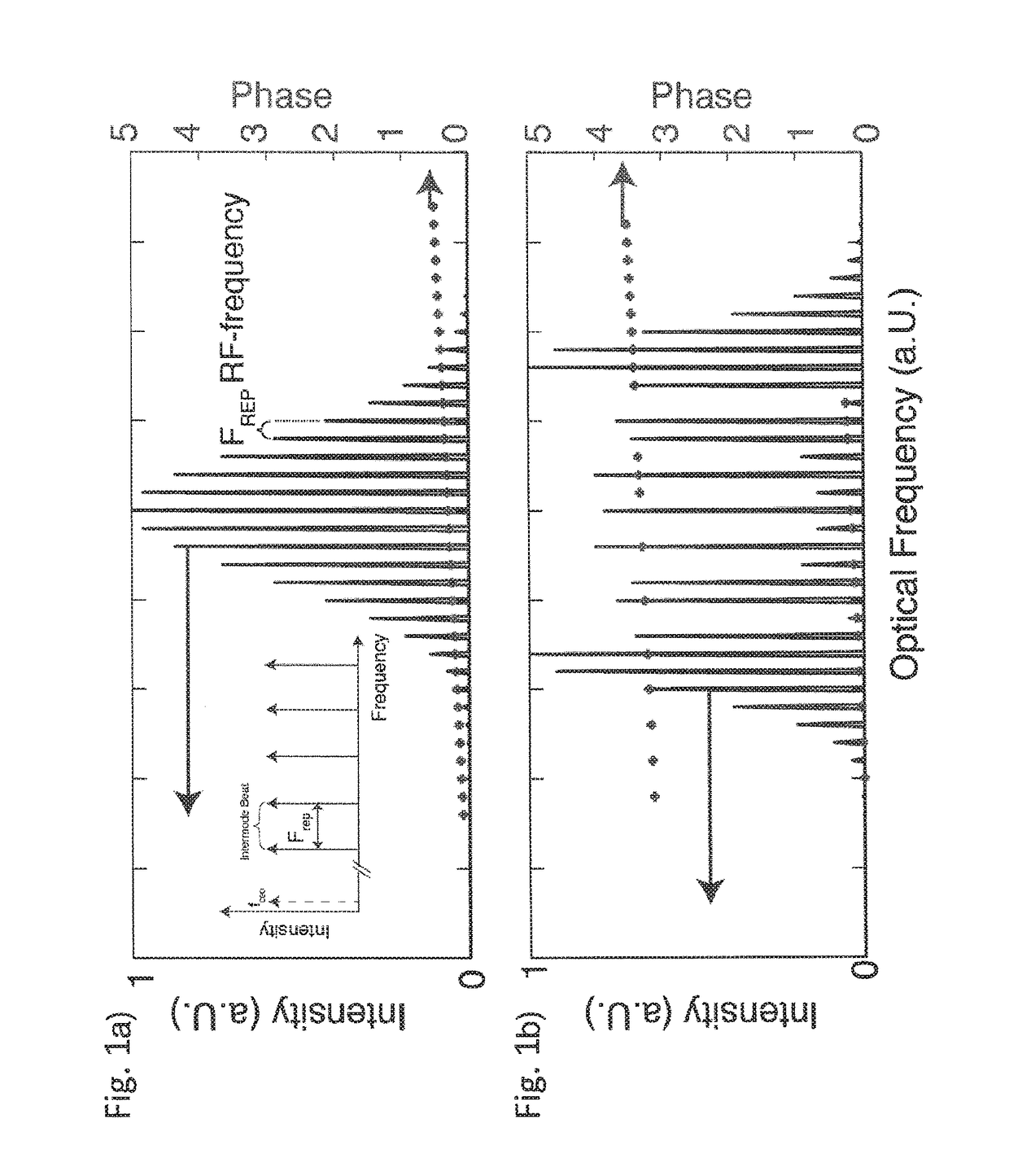
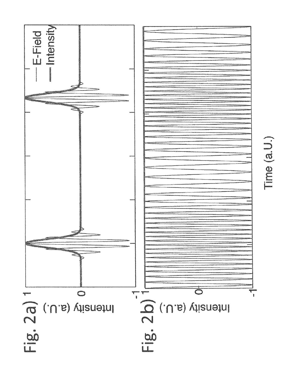
[0054]FIG. 3 shows an embodiment of an arrangement of multi-heterodyne setup. As a device setup the arrangement of FIG. 3 is known as prior art. The output of two multimode lasers and / or combs 11, 12 are combined with an optical element 13 to generate a multi-heterodyne beating within beam 15 containing the sample signal of cell 25 on the detector 20.

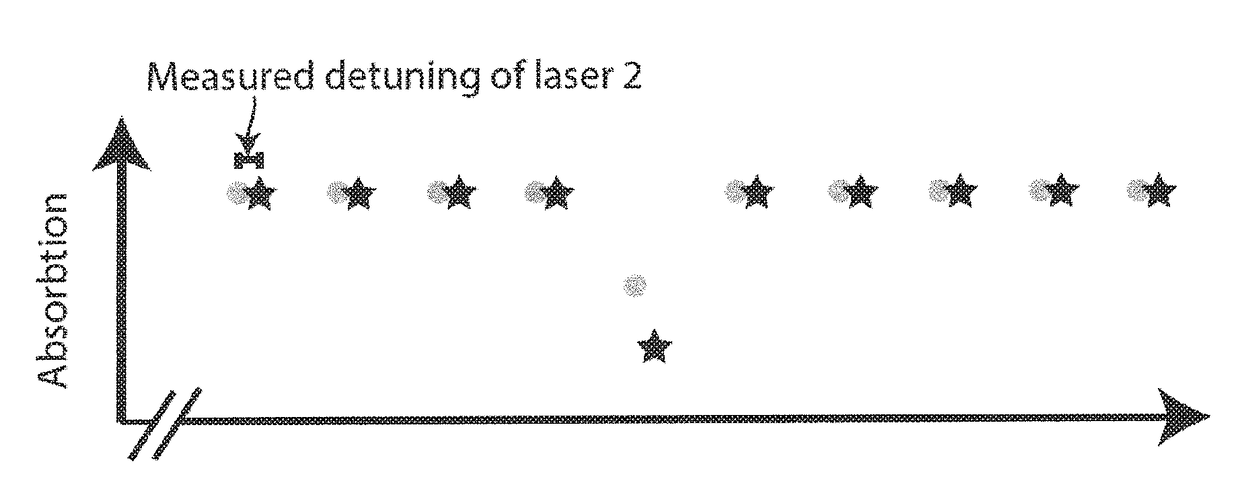
[0055]Such a multi-heterodyne system is built with at least two semiconductor multi-mode sources 11 and 12. A multi-heterodyne spectrometer is based on the readout of the amplitudes and / or relative phases and or frequencies of a multi-heterodyne signal in the RF-domain. This readout gives information about the sample in question. The information includes phase, absorption and emission. As an example, it allows to do spectroscopy. It is useful for optical analysis for substrate and sample analysis and identification. Other implementations include optical communications with a multi-heterodyne setup.

[0056]One possible implementation of a ...


PUM


Abstract

A method for optical and electrical signal processing of a multi-heterodyne signal generated by a multi-mode semi-conductor laser, for a system comprising two laser sources and an sample interaction unit. At least the beam of one of the laser passes through said sample interaction unit before being combined on a detector. The first laser is tuned (40=>42) by an amount keeping the tuning result within the available detector bandwidth (55). Then the second laser is roughly tuned by the same amount as the tuning of the first laser to bring back the signal to the vicinity (48) of the original place in the RF-domain and within the bandwidth (55) of the detector. The tuning steps are repeated with different value of mode spacing for reconstructing the sample spectrum and provide a high resolution image of the dip (41) absorption line (40).

Description

TECHNICAL FIELD[0001]The present invention relates to methods for optical and electrical signal processing of a semi-conductor laser and to a detection device utilizing said methods.PRIOR ART[0002]US 2007 / 086713 A1 discloses methods to build frequency standards based on mode-locked fiber lasers. Said document is related to applications based on frequency-combs. A comb source is characterized by its perfectly equal spacing of the modes in the frequency domain. The optical frequency of each mode can be characterized as fn=fceo+n*frep, with n>>1 . The coherence between individual modes ensures equal mode spacing. The full-width at half maximum FWHMbeatnote of the generated beatnote (also called intermode beat) reflects the purity of the coherence between the modes. Someone skilled in the art knows different comb regimes. The comb regime is defined by FWHMbeatnote<kHz, the comb-like regime is defined by kHz<FWHMbeatnote<MHz, the Fabry-Perot regime is defined by FWHMbeatno...

Claims


Application Information

Patent Timeline
IPC IPC(8): H04B10/64H04B10/524H04B10/50G01J3/433G01J9/02
CPCH04B10/64G01J3/433G01J9/0246G01J2003/423H04B10/505H04B10/524H04B10/504G01J3/10G01J9/04
Inventor HUGI, ANDREASFERREIRA VILLARES, GUSTAVO FILIPEFAIST, JEROME
Owner ETH ZZURICH
Why Eureka
Try Eureka