Voltage conversion circuit, display panel, and method for driving the display panel

Active Publication Date: 2017-08-10
TCL CHINA STAR OPTOELECTRONICS TECH CO LTD
View PDF5 Cites 5 Cited by
  • Summary
  • Abstract
  • Description
  • Claims
  • Application Information

AI Technical Summary

Benefits of technology

The patent is about a new display technology that reduces color shifting and improves image quality. The main pixel region and sub pixel region have opposite polarities, so the pixel voltage is smaller in the sub pixel region. The rotation angles of liquid crystal molecules in the main and sub pixel regions are also different, which ensures even distribution of brightness in space and reduces flickering. Overall, this technology helps create a more stable and high-quality display.

Problems solved by technology

However, since VA display devices use vertically rotating liquid crystals, birefringences of liquid crystal molecules differ greatly, thereby leading to a serious color shift at a large viewing angle.
In most technologies for improving color shift, reversed polarities of liquid crystals in a main pixel region and in a sub pixel region are the same, and therefore, the main pixel region and the sub pixel region of a sub pixel are not able to display an image in a same frame through opposite polarities.
Since absolute value of a pixel voltage of positive polarity and that of a pixel voltage of negative polarity are not completely symmetrical with respect to each other, each frame shows a periodical change in brightness which, in human vision, is flickers on the display panel, thereby rendering the display effect of the display panel inferior.
Though 2D1G technology enables the main pixel region and the sub pixel region to display an image in a same frame through opposite polarities, quantity of data signal lines is doubled, which further doubles quantity of pins of a drive IC, thereby increasing the cost of chip on film (COF) packaging of panels.
Besides, in order to drive the main pixel region and the sub pixel region simultaneously, structure of the drive IC will be more complex, which will also increase the manufacturing cost.

Method used


Image

  • Voltage conversion circuit, display panel, and method for driving the display panel
  • Voltage conversion circuit, display panel, and method for driving the display panel
  • Voltage conversion circuit, display panel, and method for driving the display panel

Examples


embodiment 1

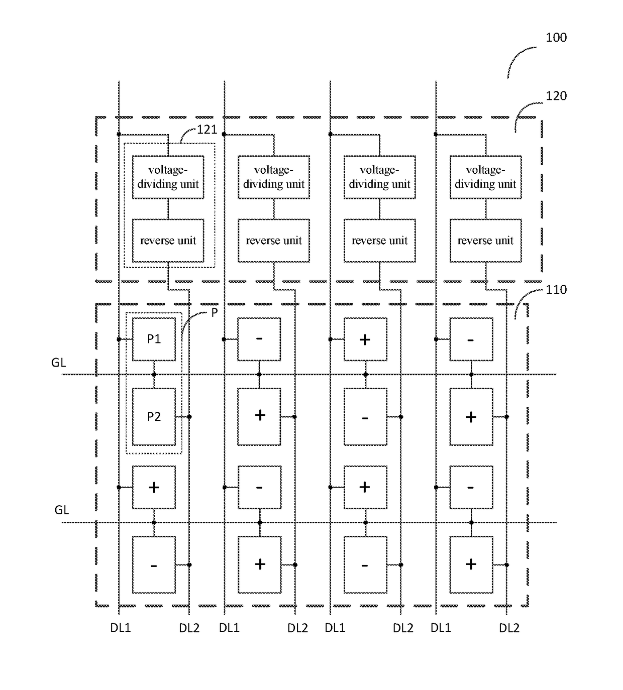
[0029]FIG. 1 schematically shows structure of a liquid crystal display panel according to the present embodiment. The display panel 100 is, for example, a vertical alignment (VA) display panel which comprises a display area 110 and a non-display area 120, wherein the non-display area 120 is located on the periphery of the display area 110. Gate lines GL and data lines DL are formed on the display panel 100 along a first direction and a second direction, respectively, and cross with each other in the display area 110. The data lines DL include a main data line DL1 and a sub data line DL2 which are parallel to each other and are arranged alternatively. The gate lines GL are used to transmit a scan drive signal. The main data line DL1 is used to transmit a data signal of a main pixel region, and the sub data line DL2 is used to transmit a data signal of a sub pixel region.

[0030]The display area 110 is provided therein with a plurality of pixel regions P. Each pixel region P is connecte...

embodiment 2

[0039]The present embodiment provides a specific structure of a voltage reversal circuit. As shown in FIG. 4, the reverse unit comprises four transistors T1, T2, T3, and T4 of a same channel type, and a capacitor C3.

[0040]The transistor T1 serves as a specific example of the sampling voltage switch;

[0041]the transistor T2 serves as a specific example of the reference voltage switch; the transistor T3 serves as a specific example of the output voltage switch; and the transistor T4 serves as a specific example of the initializing switch. The four transistors T1, T2, T3, and T4 can each be, for example, n-type thin film transistors (TFT).

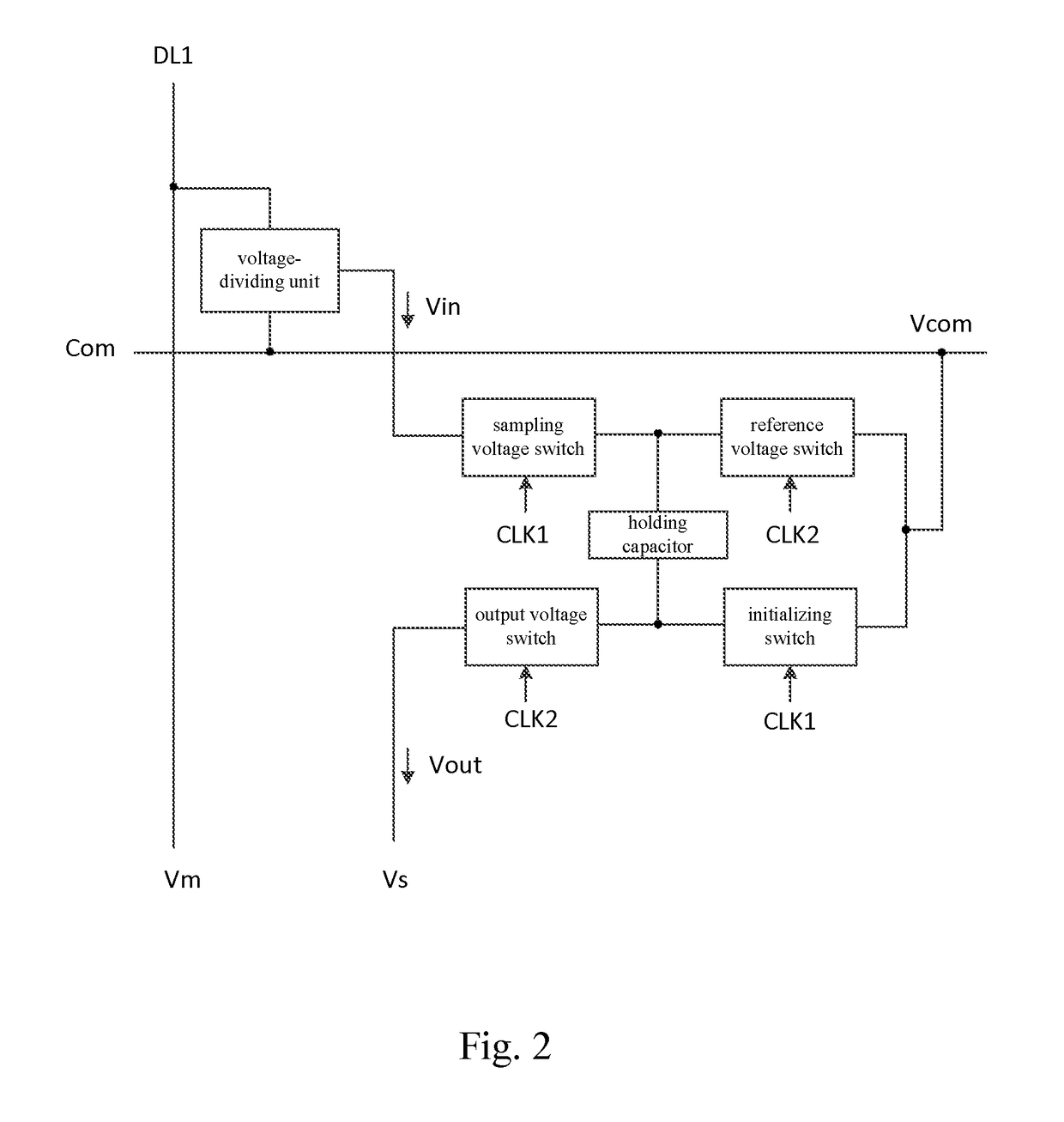
[0042]In the present embodiment, the voltage-dividing unit comprises two capacitors C1 and C2 which are in series connection. An input end of the first voltage-dividing capacitor C1 is connected to the main data line DL1, for receiving the voltage Vm of the data signal of the main pixel region. An input end of the second voltage-dividing capacitor C2 i...

embodiment 3

[0059]Different from embodiment 2, in the present embodiment two transistors T1′ and T4′ are added to the sampling voltage switch and the initializing switch. As shown in FIG. 5, a gate and a source of T1′ are short-circuited, and are coupled to a first clock source, for receiving a first clock signal CLK1. A drain of T1′ is coupled with the gate of T1′. A gate and a source of T4′ are short-circuited, and are coupled to the first clock source, for receiving the first clock signal CLK1. A drain of T4′ is coupled with the gate of T4′.

[0060]The transistors T1′ and T4′ enable the reverse unit to work more steadily. Specifically, during time period t1, when the first clock signal CLK1 jumps from a low level to a high level, the sampling voltage switch and the initializing switch can be switched on quickly, and when the first clock signal CLK1 jumps from a high level to a low level, the sampling voltage switch and the initializing switch can be switched off quickly.

[0061]Anyone skilled in...


PUM


Abstract

Disclosed is a voltage conversion circuit, display panel, and method for driving the display panel. The voltage conversion circuit comprises: a voltage-dividing unit which receives a voltage of a data signal of a main pixel region, and divides the voltage of the data signal of the main pixel region so as to output an intermediate voltage, and a reverse unit which, under control of a first clock signal and a second clock signal, inversely converts the intermediate voltage to a voltage of the data signal of a sub pixel region, rendering polarity of a pixel voltage of the sub pixel region and polarity of a pixel voltage of the main pixel region opposite to each other.

Description

CROSS-REFERENCE TO RELATED APPLICATIONS[0001]The present application claims benefit of Chinese patent application CN201510098114.9, entitled “Voltage conversion circuit, display panel, and method for driving the display panel” and filed on Mar. 5, 2015, the entirety of which is incorporated herein by reference.TECHNICAL FIELD[0002]The present disclosure relates to the technical field of liquid crystal displays, and in particular, to a voltage conversion circuit, a display panel, and a method for driving the display panel.TECHNICAL BACKGROUND[0003]In the existing technologies, liquid crystal display (LCD) devices are a type of commonly used flat-panel display device. In LCD devices, the light filed intensity of the backlight source is modulated through a liquid crystal switch, thereby achieving display of images. LCD devices have various display modes, among which is a commonly used vertical alignment (VA) display mode. VA display devices have excellent characteristics such as high c...

Claims


Application Information

Patent Timeline
IPC IPC(8): G09G3/36
CPCG09G3/3696G09G3/3614G09G2320/0247G09G2310/08G09G2330/02G09G3/3655G09G3/3688G02F1/13624G09G2320/0219G09G2320/0242G02F1/134354
Inventor XU, HONGYUAN
Owner TCL CHINA STAR OPTOELECTRONICS TECH CO LTD
Why Eureka
Try Eureka