Manufacturing method of wafer level package structure

Active Publication Date: 2017-08-10
POWERTECH TECHNOLOGY
View PDF0 Cites 2 Cited by
  • Summary
  • Abstract
  • Description
  • Claims
  • Application Information

AI Technical Summary

Benefits of technology

[0010]The invention provides a manufacturing method of a wafer level pa

Problems solved by technology

However, if the flatness of the wafer support system 11 is worse, the required height of the conductive pillars 24 or the RDL 40 is

Method used


Image

  • Manufacturing method of wafer level package structure
  • Manufacturing method of wafer level package structure
  • Manufacturing method of wafer level package structure

Examples


Embodiment Construction

[0032]In the following detailed description, for purposes of explanation, numerous specific details are set forth in order to provide a thorough understanding of the disclosed embodiments. It will be apparent, however, that one or more embodiments may be practiced without these specific details. In other instances, well-known structures and devices are schematically shown in order to simplify the drawing.

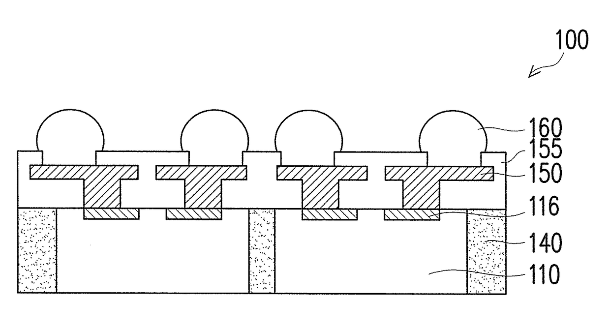
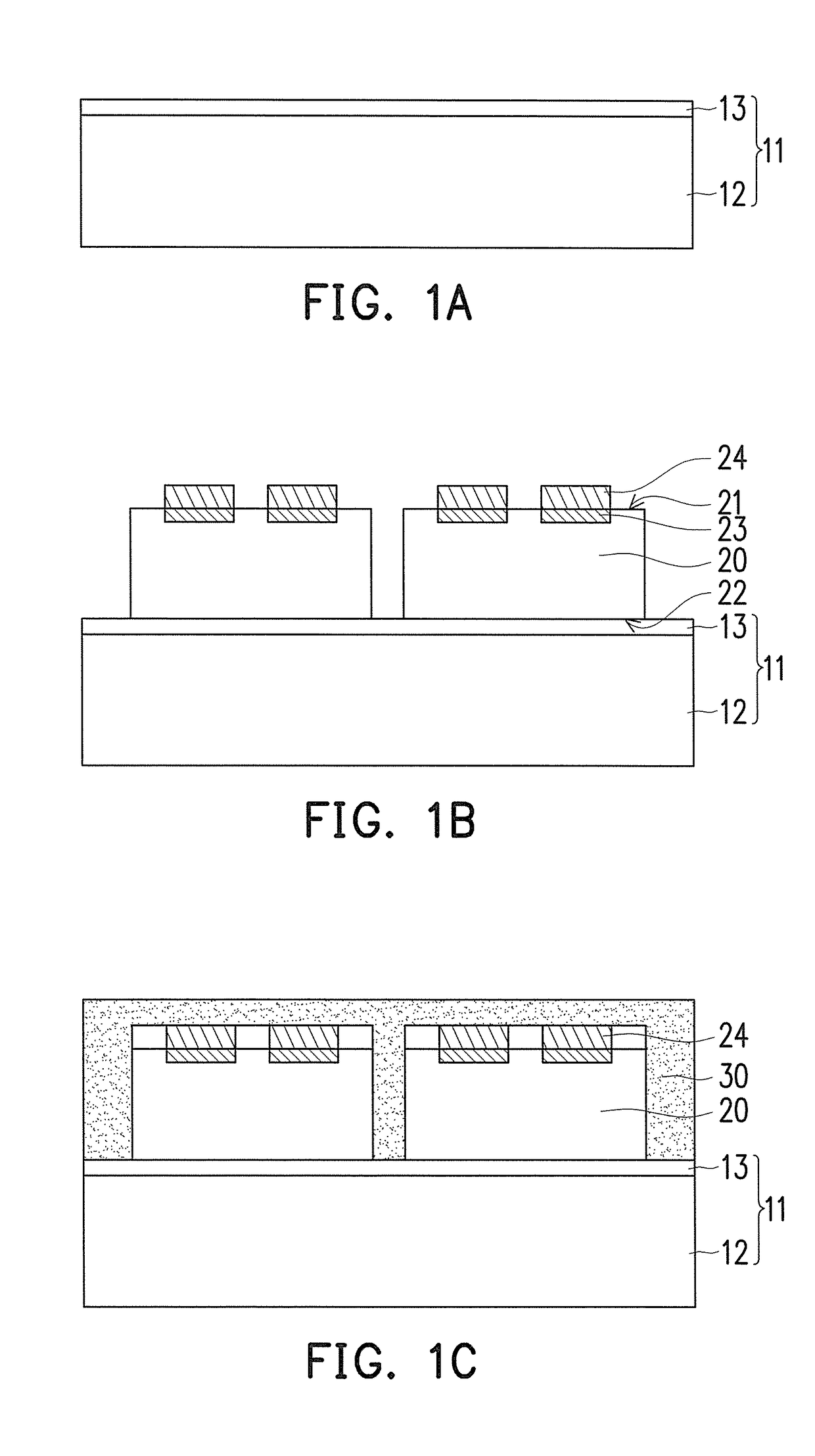
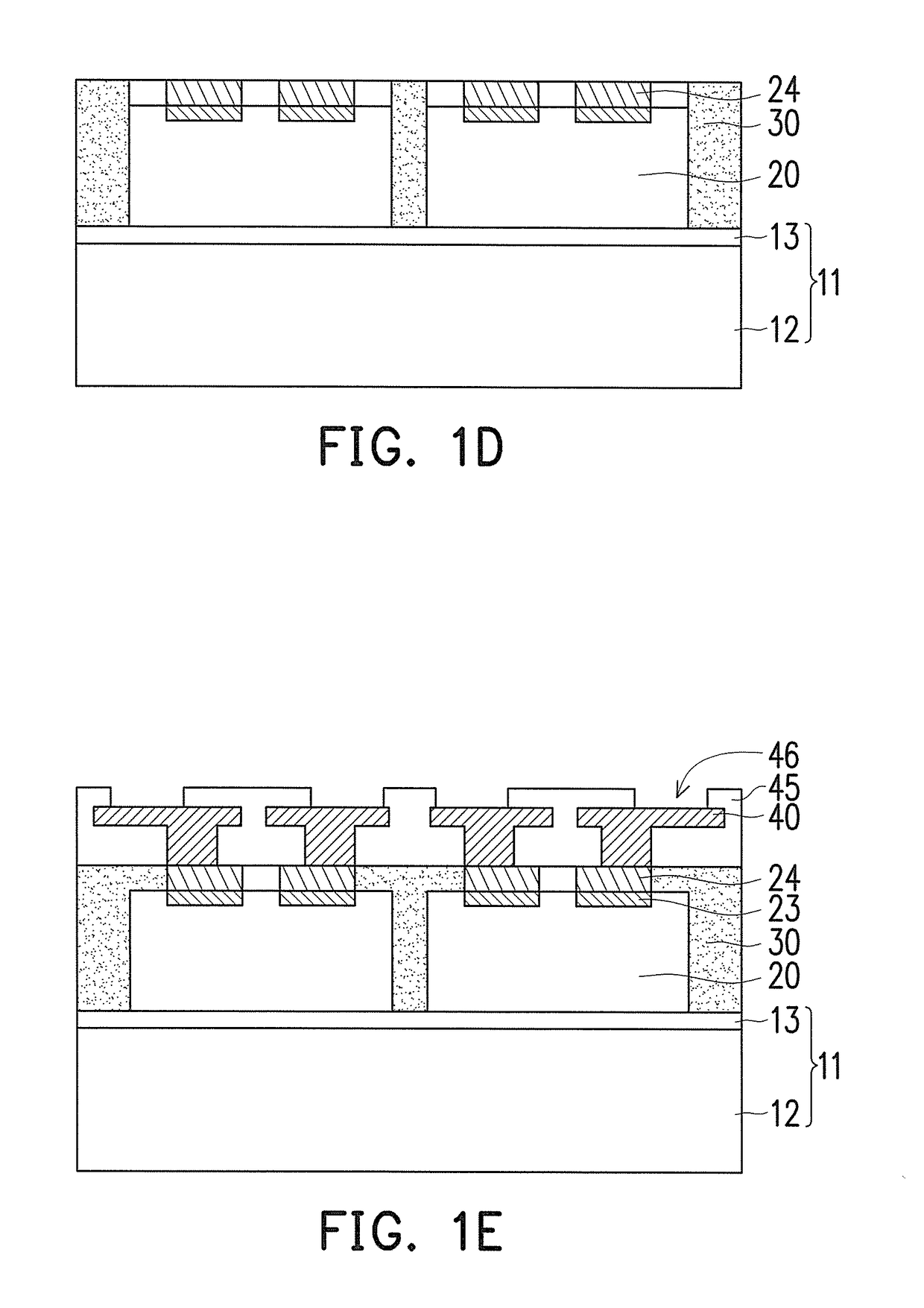
[0033]FIG. 2A to FIG. 2F are schematic diagrams of a manufacturing process of a wafer level package structure according to an embodiment of the invention. FIG. 3 is a flow diagram of a manufacturing process of a wafer level package structure according to an embodiment of the invention. Referring to FIG. 2A and FIG. 3, a manufacturing process of a wafer level package structure 200 of the embodiment includes the following steps. First, a chip 110 is provided. The chip 110 includes an active surface 112, a back surface 114 opposite to the active surface 112, and a plurality of pads 116...


PUM


Abstract

A manufacturing method of a wafer level package structure includes the following steps. A chip is disposed on a supporting board, wherein the chip includes an active surface and a back surface opposite to the active surface, and a plurality of pads on the active surface, and the back surface of the chip is adhered to the supporting board through a die attach film (DAF). A molding is disposed on the supporting board to perform a wafer level exposed die molding procedure on the chip, wherein the molding surrounds the chip, and the pads of the chip are exposed out of the molding. A redistribution layer (RDL) is formed on the active surface of the chip, wherein the RDL is electrically connected to the pads. The supporting board and the DAF are removed from the chip.

Description

CROSS-REFERENCE TO RELATED APPLICATION[0001]This application claims the priority benefit of Taiwan application serial no. 105104081, filed on Feb. 5, 2016. The entirety of the above-mentioned patent application is hereby incorporated by reference herein and made a part of this specification.BACKGROUND OF THE INVENTION[0002]Field of the Invention[0003]The invention relates to a manufacturing method of a package structure, and particularly relates to a manufacturing method of a wafer level package structure.[0004]Description of Related Art[0005]In a manufacturing process of a wafer level package (e.g., fan out wafer level package (FO-WLP)), in order to support the wafer after thinning, the wafer is usually placed on a wafer support system (WSS). In this way, the wafer is able to withstand various transport in the manufacturing process and avoid wafer warpage which may cause fragmentation.[0006]FIG. 1A to FIG. 1G are schematic diagrams of a manufacturing process of a conventional wafer...

Claims


Application Information

Patent Timeline
IPC IPC(8): H01L23/00H01L21/56
CPCH01L24/96H01L21/565H01L21/568H01L2224/13024H01L24/13H01L2224/02379H01L24/02H01L24/03H01L24/11H01L2224/03002H01L2224/04105H01L2224/05548H01L2224/05567H01L2224/11002H01L2224/12105H01L2224/13022H01L2224/131H01L2224/96H01L2924/18162H01L2924/3511H01L2224/03H01L2224/11H01L2924/014
Inventor CHANG, CHIA-HANG
Owner POWERTECH TECHNOLOGY
Why Eureka
Try Eureka