Organic Light-Emitting Device

a light-emitting device and organic technology, applied in the field of organic light-emitting devices, can solve the problems of unsatisfactory reduction of color rendering index (cri), increase in required operating voltage, and special manufacturing, and achieve the effect of avoiding scattering of light at any edge or step of inhomogeneity layer, facilitating extensive radiation of light generated in at least one organic light-emitting layer, and softer transitions

Active Publication Date: 2017-08-10
DOLYA HOLDCO 5 LTD
View PDF7 Cites 2 Cited by
  • Summary
  • Abstract
  • Description
  • Claims
  • Application Information

AI Technical Summary

Benefits of technology

[0013]According to at least one embodiment of the device, it is provided that the thickness of the inhomogeneity layer varies continuously. The thickness of the inhomogeneity layer can vary gradually, for example. The thickness preferably varies in each step of 5 nm in a lateral direction by less than 5 nm, preferably by less than 2 nm, especially preferably by less than 1 nm. Due to such a gradual, continuous and steady layer thickness progression, softer transitions are achieved between the spectral portions emitted by the different sub-regions of the device. Scattering of the light at any edges or steps of the inhomogeneity layer is also prevented.
[0014]The electrode surfaces can be formed on a large scale in each case. Extensive radiation of the light generated in the at least one organic light-emitting layer can be facilitated by this—in particular in contrast to a display in which the electrode surfaces are structured. “Large scale” can mean here that the electrode surfaces have an area of greater than or equal to one square millimeter, preferably greater than or equal to one square centimeter and especially preferably greater than or equal to one square decimeter.

Problems solved by technology

This can result in an undesirable reduction in the Color Rendering Index (CRI).
The manufacture is particularly elaborate, however, and can only be realized by the use of a cluster device.
As well as this, such a procedure is accompanied by a rise in the required operating voltage.

Method used


Image

  • Organic Light-Emitting Device
  • Organic Light-Emitting Device
  • Organic Light-Emitting Device

Examples


Embodiment Construction

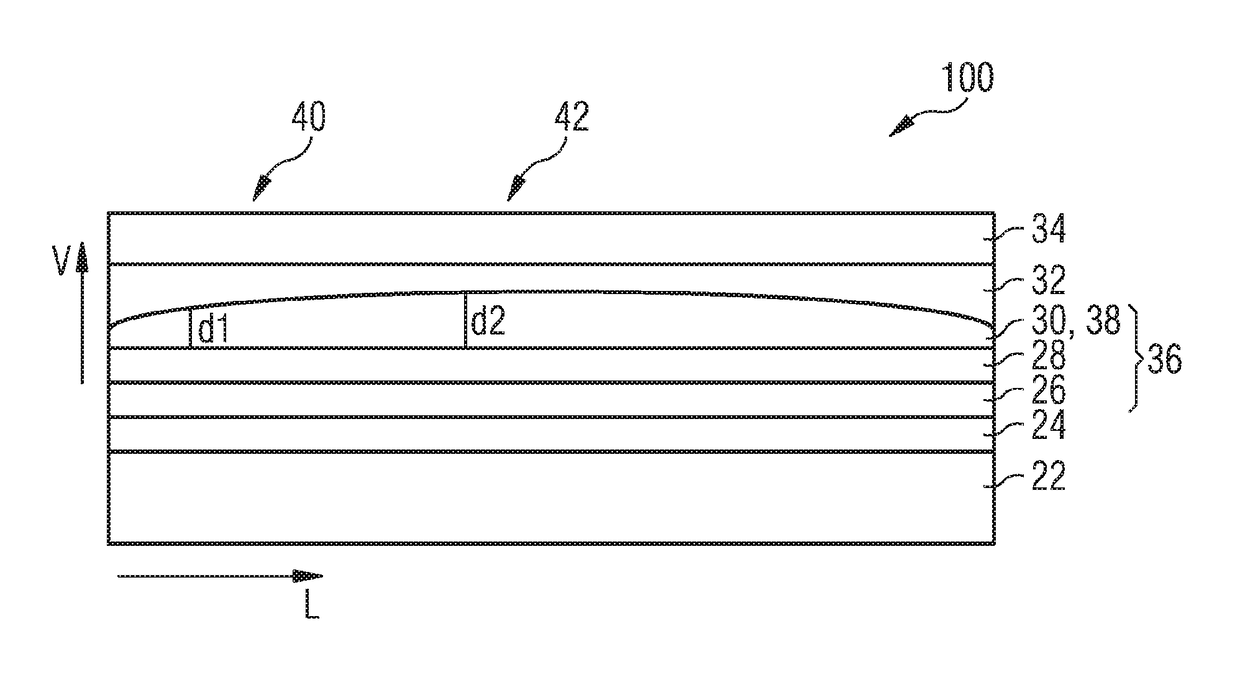
[0054]To understand the effect of the inhomogeneity layer provided according to the invention, the influence of the layer thickness of one of the layers arranged in the layer stack of an OLED, in this case the electron transport layer (ETL), on the light radiated by the device is shown in FIG. 1. The results of a simulation are shown in which an intensity of the light radiated by a device was calculated as a function of the emitted wavelength, wherein the device has an electron transport layer of a constant thickness.

[0055]The curve designated 10 represents the intensity curve in a device with an 80 nm thick electron transport layer. By comparison with this, the curve 12 represents the intensity curve in the case of an otherwise identically constructed device in which the thickness of the electron transport layer is 50 nm. It is clear that the two curves 10, 12 have maxima and minima at different wavelengths, wherein the maxima also exhibit different widths. In addition, in FIG. 1 t...


PUM


Abstract

An organic light-emitting device and a method for producing an organic light emitting device are disclosed. In an embodiment the device includes a substrate and at least one layer sequence arranged on the substrate and suitable for generating electromagnetic radiation. The at least one layer sequence includes at least one first electrode surface arranged on the substrate, at least one second electrode surface arranged on the first electrode surface and an organic functional layer stack having organic functional layers between the first electrode surface and the second electrode surface. The organic functional layer stack includes at least one organic light-emitting layer, wherein the at least one organic light-emitting layer is configured to emit light, wherein the organic functional layer stack includes at least one inhomogeneity layer, and wherein a thickness of the at least one inhomogeneity layer varies in a lateral direction.

Description

[0001]This patent application is a national phase filing under section 371 of PCT / EP2015 / 053417, filed Feb. 18, 2015, which claims the priority of German patent application 10 2014 102 191.6, filed Feb. 20, 2014, each of which is incorporated herein by reference in its entirety.TECHNICAL FIELD[0002]An organic light-emitting device is specified.BACKGROUND[0003]In organic light-emitting diodes (OLEDs) only a portion of the light generated is outcoupled directly. The remaining light produced in the active region is distributed to different loss channels, thus in light, for instance, which is carried in the substrate, in a transparent electrode and in organic layers due to waveguide effects, and in surface plasmons, which can be produced in a metal electrode. The waveguide effects occur in particular due to the differences in the refractive index at the boundaries between the individual layers and regions of an OLED. In known OLEDs only roughly a quarter of the light generated in the ac...

Claims


Application Information

Patent Timeline
Patent Type & Authority Applications(United States)
IPC IPC(8): H01L51/52H01L51/56H01L51/00H01L51/50
CPCH01L51/504H01L51/5056H01L51/5072H01L51/56H01L51/5221H01L2251/558H01L51/5265H01L51/5206H01L51/0011H10K50/15H10K50/16H10K50/80H10K71/00H10K50/852H10K2102/351H10K50/13H10K50/81H10K50/82H10K71/166
Inventor RIEDEL, DANIELWEHLUS, THOMASDIEZ, CAROLARIEGEL, NINANIEDERMEIER, ULRICHFLEI NER, ARNELANG, ERWIN
Owner DOLYA HOLDCO 5 LTD
Why Eureka
Try Eureka