Magnetometer

a magnetometer and refraction technology, applied in the field of magnetometers, can solve the problems of increasing the size of various kinds of devices formed

Active Publication Date: 2017-08-17
RENESAS ELECTRONICS CORP
View PDF5 Cites 26 Cited by
  • Summary
  • Abstract
  • Description
  • Claims
  • Application Information

AI Technical Summary

Benefits of technology

[0014]According to the above-described one embodimen

Problems solved by technology

This causes a problem of increasing a size of variou

Method used


Image

  • Magnetometer
  • Magnetometer
  • Magnetometer

Examples


first embodiment

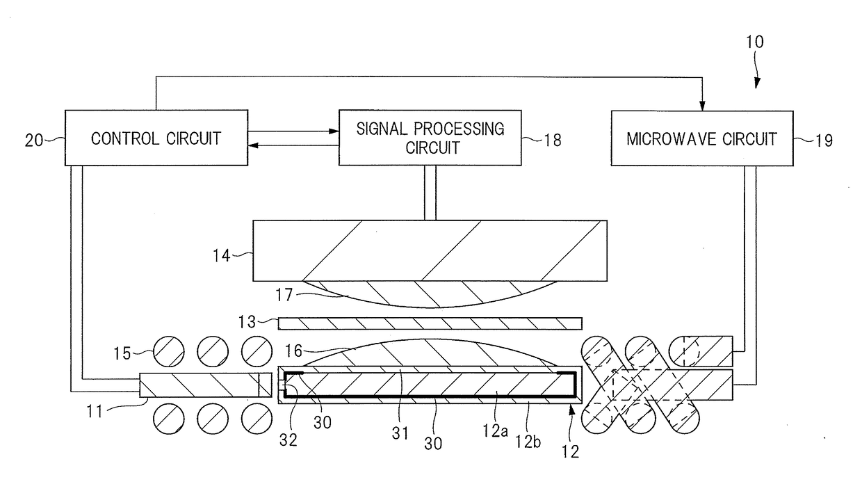
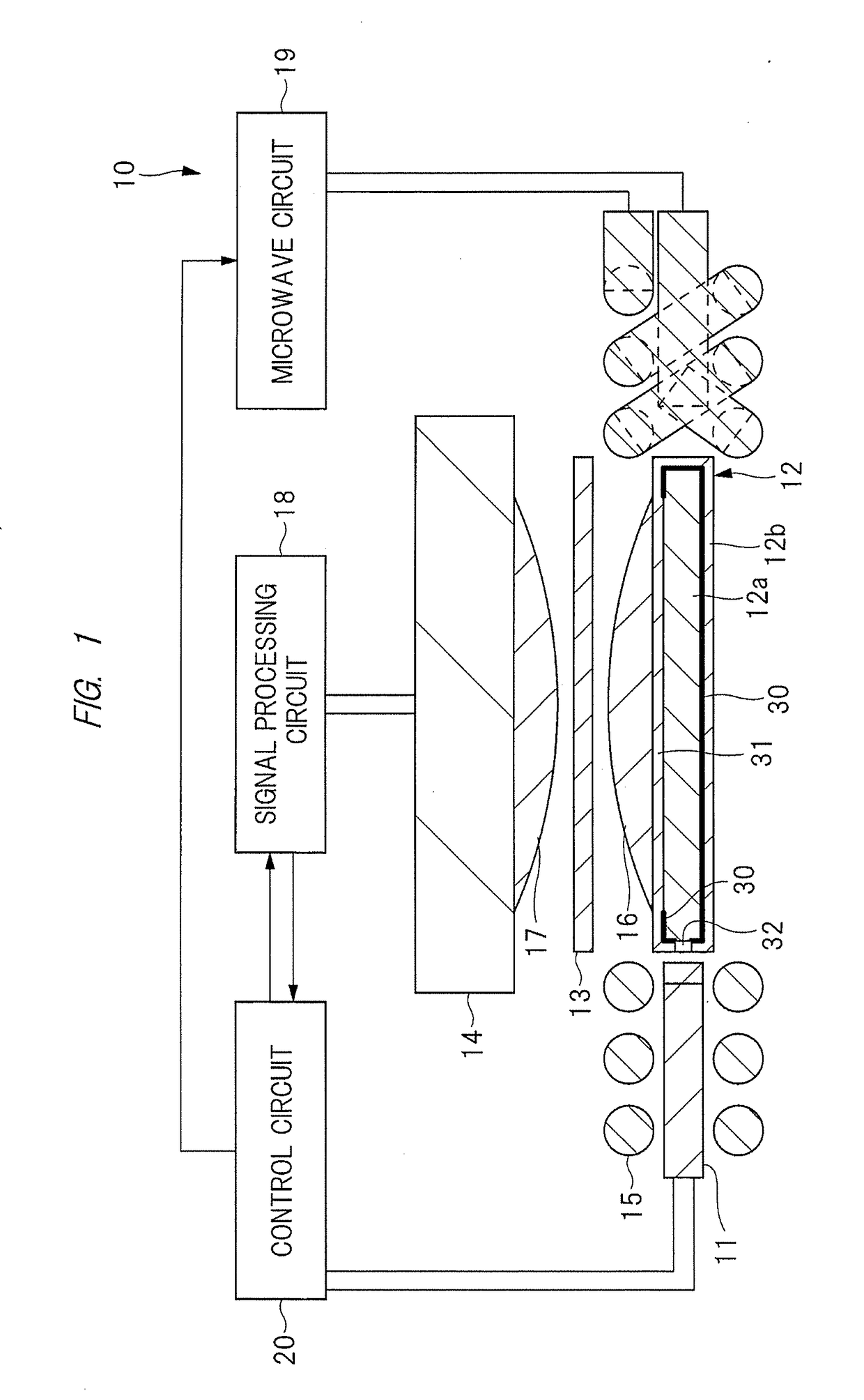
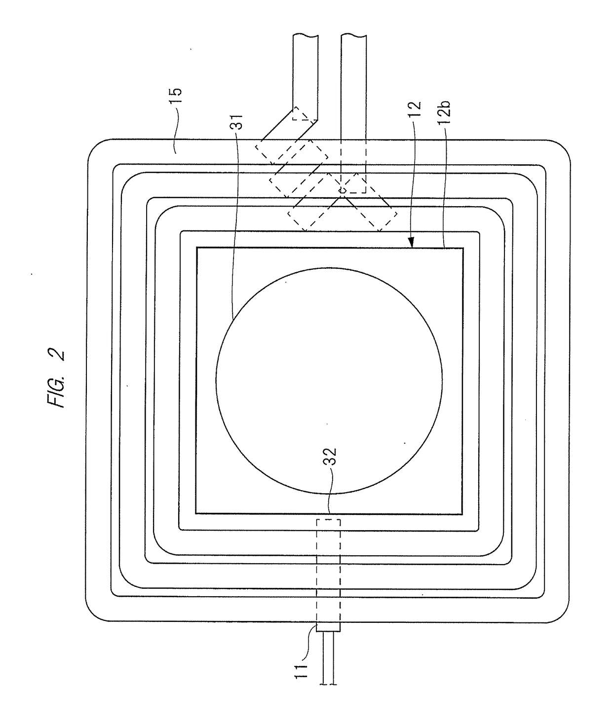
[0057]FIG. 1 is an explanatory drawing showing an example of a structure of a magnetometer according to a first embodiment. FIG. 2 is a plan view of a diamond sensor unit and a microwave coil included in the magnetometer shown in FIG. 1.

[0058]A magnetometer 10 has a module package structure, and the magnetometer 10 is made thinner and smaller. As shown in FIG. 1 and FIG. 2, the magnetometer 10 includes an excitation light source 11, a diamond sensor unit 12, a low-pass filter 13, a photodiode 14, a microwave coil 15, lenses 16 and 17, a signal processing circuit 18, a microwave circuit 19, and a control circuit 20.

[0059]The lens 16 which is a first lens is provided on the diamond sensor unit 12. More specifically, the lens 16 is provided on a fluorescence output window 31 formed in a diamond sensor case 12b described later.

[0060]The low-pass filter 13 is provided above the lens 16 at a certain distance from the lens 16. The photodiode 14 which is a fluorescence intensity detecting u...

second embodiment

[0120]In the structure according to the first embodiment described above, excitation light is incident from a side surface of the diamond sensor case 12b. Meanwhile, a technique for allowing excitation light to be incident obliquely from above the diamond sensor case 12b will be described in the second embodiment.

[0121]FIG. 6 is an explanatory drawing showing an example of across section of the magnetometer 10 according to the second embodiment. FIG. 7 is a plan view of FIG. 6. Note that the signal processing circuit 18, the microwave circuit 19, and the control circuit 20 are omitted for simplification in FIG. 6 and FIG. 7.

[0122]A difference between the magnetometer 10 shown in FIG. 6 and the magnetometer 10 in FIG. 1 according to the first embodiment described above lies in that excitation light from the excitation light source 11 is not incident on a side surface of the diamond sensor case 12b, but incident obliquely from above a back surface of the diamond sensor case 12b, which...

third embodiment

[0135]The magnetometer 10 according to the first embodiment described above has a structure in which one lens is provided for one diamond sensor unit 12. Meanwhile, a case in which a plurality of lenses are provided for one diamond sensor unit 12 will be described in the third embodiment.

[0136]FIG. 8 is an explanatory drawing showing an example of a cross section of the magnetometer 10 according to the third embodiment. FIG. 9 is a plan view of FIG. 8. FIG. 9 is a plan view of the magnetometer 10 viewed from a magnetism measurement surface, that is, a main surface of the diamond sensor 12a. Note that the signal processing circuit 18, the microwave circuit 19, and the control circuit 20 are omitted for simplification in FIG. 8 and FIG. 9.

[0137]A difference between the magnetometer 10 shown in FIG. 8 and FIG. 9 and the magnetometer 10 in FIG. 1 and FIG. 2 according to the above-described first embodiment lies in that each of the lenses 16 and 17 is not formed of a single lens, but is ...


PUM


Abstract

A magnetometer includes a diamond sensor, an excitation light source, a diamond sensor case, and a photodiode. The excitation light source irradiates the diamond sensor case with excitation light. In the diamond sensor case, a reflection film which reflects excitation light is formed on either a front surface or an inner surface, and the diamond sensor is stored. The photodiode detects intensity of fluorescence generated from the diamond sensor. The diamond sensor case includes a fluorescence output window and an excitation-light reception window. Fluorescence generated by the diamond sensor is output through the fluorescence output window. Excitation light emitted by the excitation light source is received through the excitation-light reception window. The photodiode is provided on a side of a second surface opposite to a first surface which is a magnetism measurement surface of the diamond sensor.

Description

CROSS-REFERENCE TO RELATED APPLICATION[0001]The present application claims priority from Japanese Patent Application No. 2016-026993 filed on Feb. 16, 2016, the content of which is hereby incorporated by reference into this application.TECHNICAL FIELD OF THE INVENTION[0002]The present invention relates to a magnetometer, and particularly relates to an effective technique in miniaturizing a highly-sensitive magnetic sensor using nitrogen-vacancy centers of a diamond crystal.BACKGROUND OF THE INVENTION[0003]For a highly-sensitive magnetometer which is operable at a room temperature, a diamond crystal including nitrogen-vacancy centers (NV centers) has been proposed (see, for example, D. Sage et al., “Efficient photon detection from color centers in a diamond optical waveguide” PHYSICAL REVIEW B 85, 121202(R) (2012) (Non-Patent Document 1)).[0004]The Non-Patent Document 1 discloses that, by detecting fluorescence generated from a diamond crystal while irradiating the diamond crystal wi...

Claims


Application Information

Patent Timeline
IPC IPC(8): G01N21/64G01V3/02
CPCG01R33/032A61B5/0071G01R33/1284
Inventor HATANO, YUJIYOSHINO, TAKASHI
Owner RENESAS ELECTRONICS CORP
Why Eureka
Try Eureka