Optical proximity sensor arrangement and method for producing an optical proximity sensor arrangement

a technology of optical proximity sensor and optical proximity sensor, which is applied in the direction of wave based measurement system, using reradiation, instruments, etc., can solve the problems of optical crosstalk and still be problematic in the final product, and achieve the effect of improving the signal-to-noise ratio and accuracy of optical proximity detection, reducing the risk of trapped charge, and improving the light gathering and sensitivity of the proximity sensor

Active Publication Date: 2017-08-31
AMS AG
View PDF31 Cites 8 Cited by
  • Summary
  • Abstract
  • Description
  • Claims
  • Application Information

AI Technical Summary

Benefits of technology

[0015]The light blocking slats are arranged to only pass light from the second region of incidence angles. In fact, the slats can be intentionally sized and oriented with the purpose of blocking offending crosstalk rays originating from reflections off of the cover. In fact, controlling specular crosstalk with layers of slats instead of with inked apertures, rubber boots, and restricted shield apertures can further improve signal-to-noise ratio and accuracy of optical proximity detection.
[0016]The slats can be distributed in the mask by defining the layers without the need of staggered walls connected by vias, for example. Vias, like through-substrate-vias, are optional structures and can be used to ground the slats or layers to reduce the risk of trapped charge in the sensor arrangement. Furthermore, this allows light to impinge from more directions, significantly improving the light gathering and sensitivity of the proximity sensor.
[0017]The exact size, distance and orientation of slats in the respective layer typically is a result borne out by optical simulation or ray tracing software such as TracePro or Zemax. The slat orientation allows specific targeting of the “problem” rays, i.e. it blocks specularly reflected rays coming from the cover, while otherwise opening up the angular aperture to receive light from other directions, resulting in improved optical signal and sensitivity. Tailoring the design specifically to block offending crosstalk rays allows more precise control of the package performance, as layer geometry can be controlled very precisely in fabrication at wafer level, for example. This helps alleviate problems of crosstalk caused by system level variations such as customer air gap, customer misalignment of inked apertures etc. It also results in improved light gathering efficiency. In fact, suppressing crosstalk with layered slat structures such as the suggested mask allows system apertures that were reduced and shaped to control optical crosstalk in other designs to be opened up larger.

Problems solved by technology

Optical crosstalk has always been the most significant problem for optical proximity sensors, due mainly to Fresnel reflections off of the inside and outside surfaces of glass or plastic covers that typically cover the proximity sensor in cell phone and tablet products, for example.
Even with dedicated system design, the crosstalk can still be problematic in a final product due to variations in factors such as air gap, lateral device alignment with respect to apertures and the like.

Method used


Image

  • Optical proximity sensor arrangement and method for producing an optical proximity sensor arrangement
  • Optical proximity sensor arrangement and method for producing an optical proximity sensor arrangement
  • Optical proximity sensor arrangement and method for producing an optical proximity sensor arrangement

Examples


Embodiment Construction

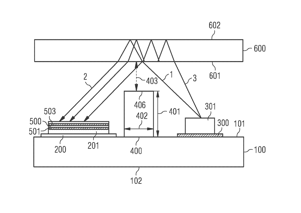
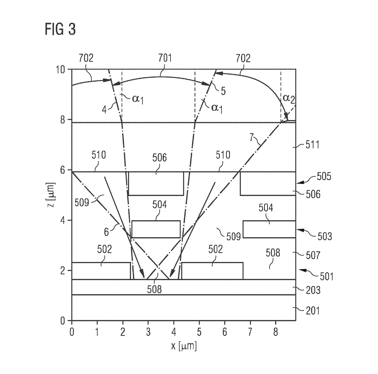
[0049]FIG. 1 shows a side view of an embodiment of an optical proximity sensor arrangement.

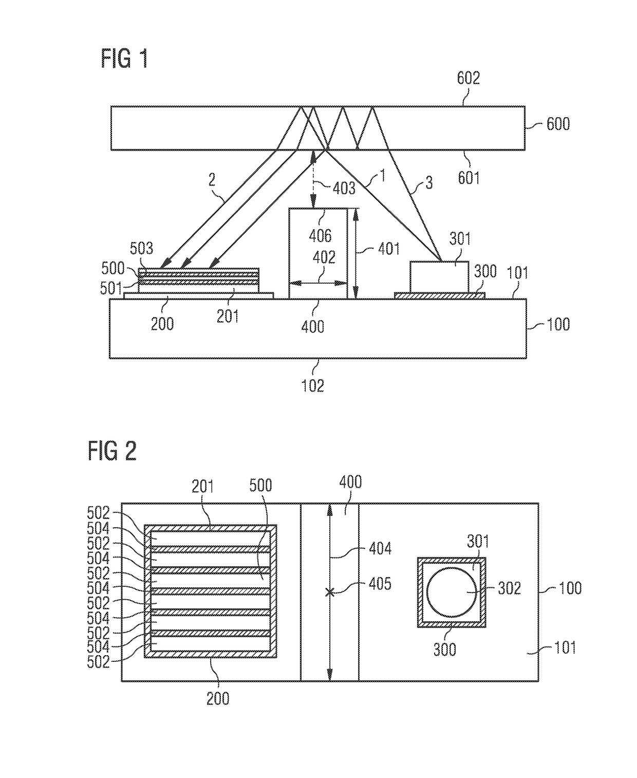
[0050]The drawing depicts an optical proximity sensor arrangement embedded in a larger device such as a smartphone or tablet. The optical sensor arrangement comprises a substrate 100 having a main surface 101 which extends into an X- and Y-direction. Arranged on the main surface 101 is a first integrated circuit 200, a second integrated circuit 300 and an optical light barrier 400 arranged in between these circuits. Typically, the light barrier 400 is centered with respect to a center point 405 between the first integrated circuit 200 and the second integrated circuit 300 (see FIG. 2).

[0051]The first integrated circuit 200 comprises at least one light sensitive component 201. In this particular embodiment the light sensitive component is a photodiode. The first integrated circuit 200 further comprises terminals (not shown) for electrically connecting the photodiode through the substrate 100. F...


PUM


Abstract

An optical proximity sensor arrangement comprises a semiconductor substrate (100) with a main surface (101). A first integrated circuit (200) comprises at least one light sensitive component (201). The first integrated circuit is arranged on the substrate at or near the main surface. A second integrated circuit (300) comprises at least one light emitting component (301), and is arranged on the substrate at or near the main surface. A light barrier (400) is arranged between the first and second integrated circuits. The light barrier being designed to block light to be emitted by the at least one light emitting component from directly reaching the at least one light sensitive component. A multilayer mask (500) is arranged on or near the first integrated circuit and comprising a stack (501) of a first layer (502) of first elongated light blocking slats (503) and at least one second layer (504) of second elongated light blocking slats (505). The light blocking slats are arranged in the mask to block light, incident on the mask from a first region of incidence (701), and to pass light, incident on the mask from a second region of incidence (702), from reaching the at least one light sensitive component.

Description

CROSS-REFERENCE TO RELATED APPLICATION[0001]This application claims priority to European Patent Application No. 16160935.9, filed Mar. 17, 2016, and to U.S. Provisional Patent Application No. 62 / 300,203, filed Feb. 26, 2016, all of which are hereby incorporated by reference in their entirety for all purposes.[0002]The following relates to an optical proximity sensor arrangement and to a method for producing an optical proximity sensor arrangement.BACKGROUND OF THE INVENTION[0003]Optical proximity sensors are active sensors that are used to detect the presence or distance of an object within their measuring range. Typically an optical proximity sensor comprises a light source to emit light towards an object, and an optical sensor that detects the amount of light which eventually gets reflected back from the object. The light source generates visual, infrared or ultraviolet (UV) light depending on the spectral sensitivity of sensor. Typically, the light source is chosen to emit light ...

Claims


Application Information

Patent Timeline
Patent Type & Authority Applications(United States)
IPC IPC(8): H01L25/16G01S17/02H01L31/167G01S7/481H01L31/0216H01L31/0232G01S17/04
CPCH01L25/167H01L25/165H01L31/02162G01S17/02H01L31/167G01S7/4811H01L31/02327G01S7/4813G01S17/04
Inventor MEHRL, DAVIDSTOLTZ, GREG
Owner AMS AG
Why Eureka
Try Eureka