
Method for fabricating ceramic insulator for electronic packaging

a ceramic insulator and electronic packaging technology, applied in the direction of printed circuit aspects, printed element electric connection formation, semiconductor/solid-state device details, etc., can solve the problems of affecting the appearance and reliability of porcelain (ceramic), reducing the density and bonding strength of the coating layer, and unable to meet the ever-increasing requirements of high-performance products. , to achieve the effect of improving the overall performance of the porcelain and improving the quality of the coating layer

Active Publication Date: 2017-09-07
HEBEI SINOPACK ELECTRONICS TECH
View PDF13 Cites 0 Cited by
  • Summary
  • Abstract
  • Description
  • Claims
  • Application Information

AI Technical Summary

Benefits of technology

The method achieves a high-quality nickel alloy coating with improved reliability and appearance, enabling effective electrical connections and enhanced overall performance of the ceramic insulator.

Problems solved by technology

However, after the electroplating is realized by the connection using the bonding wires, the metal strips need to be shoveled; thus, it is inevitable to remain shoveling traces on the circuits, and thereby affect appearance and reliability of the porcelain (ceramic).
In addition, compared with the electroplating method, the adoption of the chemical coating method may result in relatively lower coating layer density and bonding strength, and can't meet ever-increasing requirements of high-performance products.

Method used


Image

  • Method for fabricating ceramic insulator for electronic packaging
  • Method for fabricating ceramic insulator for electronic packaging
  • Method for fabricating ceramic insulator for electronic packaging

Examples


embodiment one

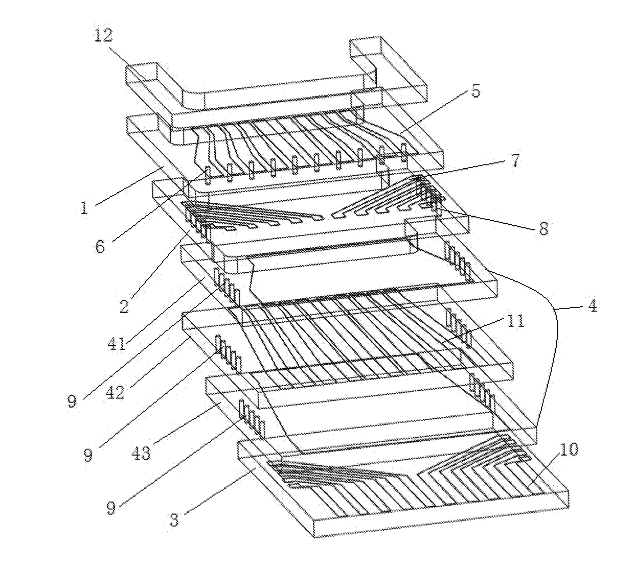
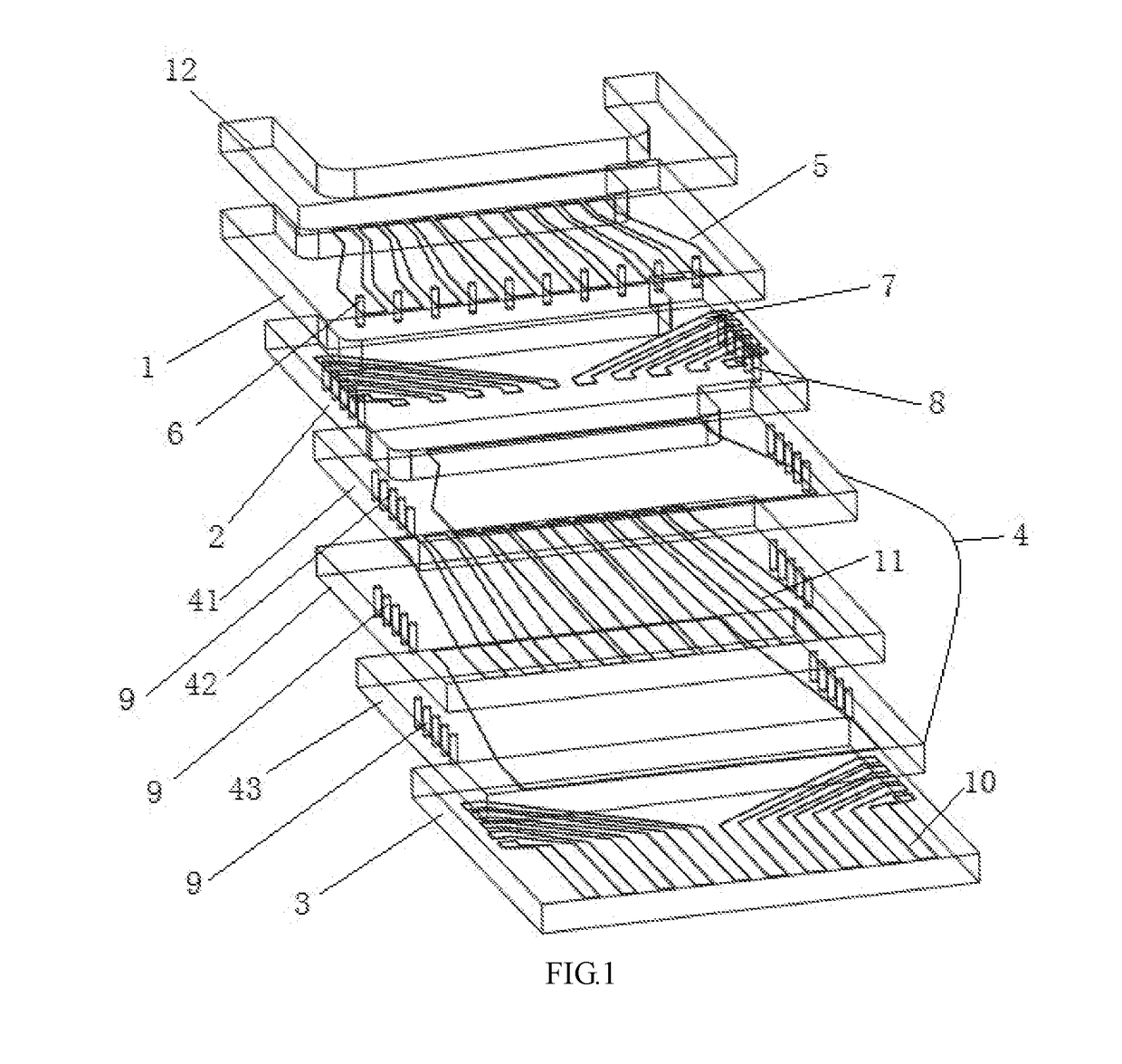
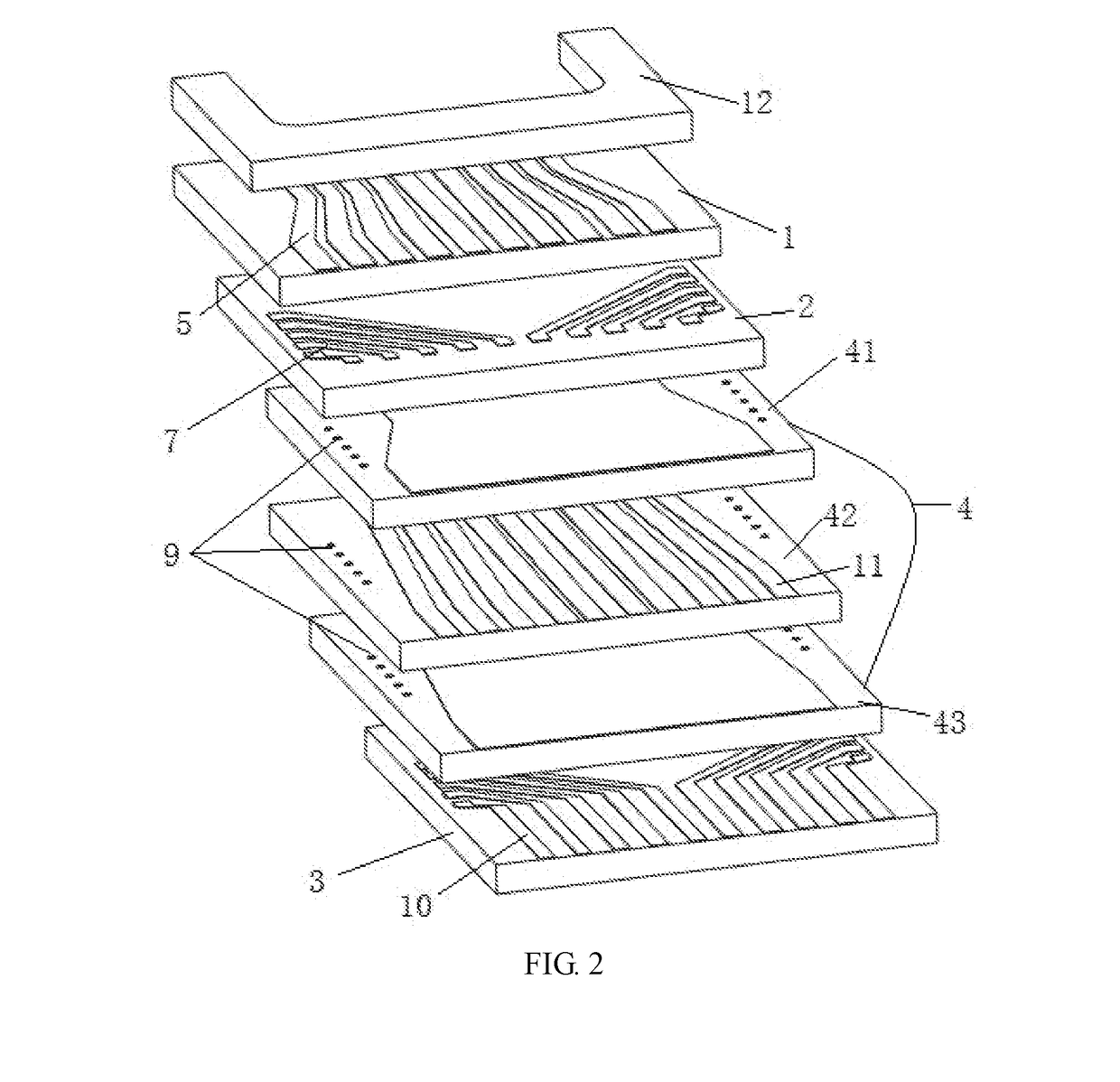
[0028]As shown in FIG. 1 and FIG. 2, the present application discloses a ceramic insulator for electronic packaging, which comprises a first ceramic layer 1, a second ceramic layer 2, an intermediate ceramic component layer 4 and a third ceramic layer 3; an upper surface of the first ceramic layer 1 is provided with a structural beam 12 configured for enhancing an overall intensity of the ceramic insulator. The upper surface of the first ceramic layer 1 is provided with an upper electric control layer, the upper electric control layer comprises a plurality of first metal strips 5 of which the number is equal to the number of the bonding pads of the insulator, the first metal strips 5 are insulated from and not interconnected with each other; positions of the first ceramic layer 1 corresponding to the positions of the bonding pads of the insulator are provided with a plurality of first via holes, each the first via hole is provided therein with a first connecting metal wire 6, the fi...

embodiment two

[0033]The present application further discloses a method for fabricating a ceramic insulator for electronic packaging, which comprises the following steps:

[0034]1) punching holes at positions of bonding pads of a first ceramic layer 1 of a ceramic insulator, metallizing and solidifying the holes, afterwards, printing an upper electric control layer circuit, the upper electric control layer circuit comprises a plurality of metal strips, the metal strips are insulated from and not interconnected with each other, but the metal strips correspond to metal in the holes one to one, and interconnect with the metal in the holes;

[0035]2) using an underside of the first ceramic layer 1 as a second ceramic layer 2, punching two groups of holes respectively on two sides of the second ceramic layer 1 corresponding to positions of the holes of the first ceramic layer 1, metallizing and solidifying the holes of the second ceramic layer 2, such that the total number of the holes at the two sides of ...


PUM

PropertyMeasurementUnit
electrical propertiesaaaaaaaaaa
conductiveaaaaaaaaaa
densityaaaaaaaaaa

Abstract

The present application discloses a method for fabricating ceramic insulator for electronic packaging, and relates to a technical field of outer shell packaging of electronic devices. Under the circumstance of using neither a chemical coating nor any bonding wire connection circuit, through a design that builds a electroplated circuit into the ceramic insulator, the method accomplishes coating of a nickel alloy protection layer onto a porcelain by an electroplating method, so that not only quality of a coating layer but also requirement of a complete appearance can be ensured. All circuits of the ceramic insulator fabricated by the aforesaid method can conduct with external circuits, such that the electroplating method can be used to accomplish coating of the nickel alloy layer, after accomplishment of all metal coating, metallization parts on an end surface of the porcelain is removed.

Description

TECHNICAL FIELD[0001]The present application relates to the technical field of outer shell packaging of electronic components, and more particularly, relates to a method for fabricating the ceramic insulator for electronic packaging.BACKGROUND[0002]A ceramic insulator is the most important component in a ceramic metal packaging outer shell, and is widely used in the photo-electronic communication field. Regarding to a ceramic insulator with a step-shaped double-deck bonding pad structure, an upper layer of the ceramic insulator is an electric control layer, a lower layer of the ceramic insulator is a RF (Radio Frequency) layer, and both the upper and lower layers need to be coated with nickel-gold protection layers so as to enhance the reliability of their structures and electrical properties.[0003]Currently, there are two methods for coating metal onto a ceramic insulator with the aforesaid structure: 1) after coating of a nickel layer on exposed metal parts of a porcelain (ceramic...

Claims


Application Information

Patent Timeline
Patent Type & Authority Applications(United States)
IPC IPC(8): H05K1/03H05K3/40H05K3/00H05K1/11H05K1/02H05K3/18
CPCH05K1/0213H05K3/4038H05K3/40H05K3/188H05K2201/09218H05K1/112H05K1/0306H05K1/0298H05K3/005H01L21/4857H01L23/13H01L23/15H01L23/49822H01L23/49838H05K1/0243H05K3/4617H05K2201/0723H05K2201/09618H05K2201/10303
Inventor ZHAO, DONGLIANGDING, FEILIU, LINJIE
Owner HEBEI SINOPACK ELECTRONICS TECH
Learn More