Power metal-oxide-semiconductor device

a technology of metal oxides and magnetic devices, applied in the direction of magnetic devices, basic electric elements, electrical equipment, etc., can solve the problems of the inability of conventional super-junction power mos devices to withstand avalanche energy, and achieve the effect of enhancing the capability of mos devices to withstand and little capability to withstand

Inactive Publication Date: 2017-09-14
BRIGHT TOWARD IND CO LTD
View PDF0 Cites 3 Cited by
  • Summary
  • Abstract
  • Description
  • Claims
  • Application Information

AI Technical Summary

Benefits of technology

[0009]As mentioned, the conventional super-junction power MOS device has little capability to withstand avalanche energy. Accordingly, a super-junction power MOS device is provided in the present invention, which features the additional breakdown-first area to enhance the capability for the MOS device to withstand avalanche energy.

Problems solved by technology

As mentioned, the conventional super-junction power MOS device has little capability to withstand avalanche energy.

Method used


Image

  • Power metal-oxide-semiconductor device
  • Power metal-oxide-semiconductor device
  • Power metal-oxide-semiconductor device

Examples


first embodiment

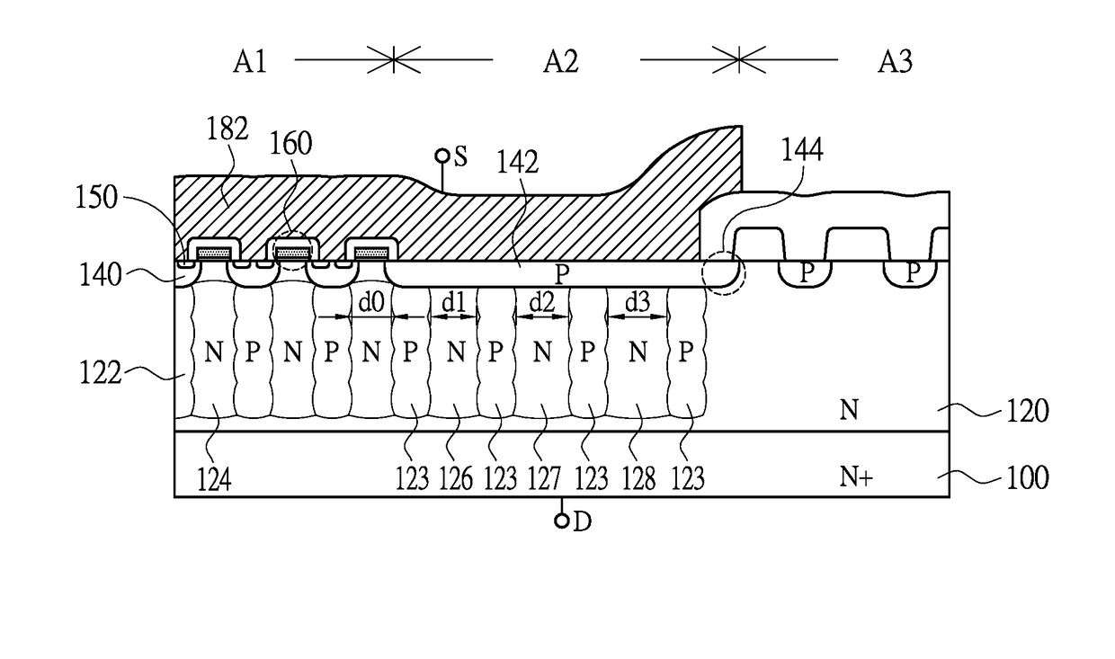
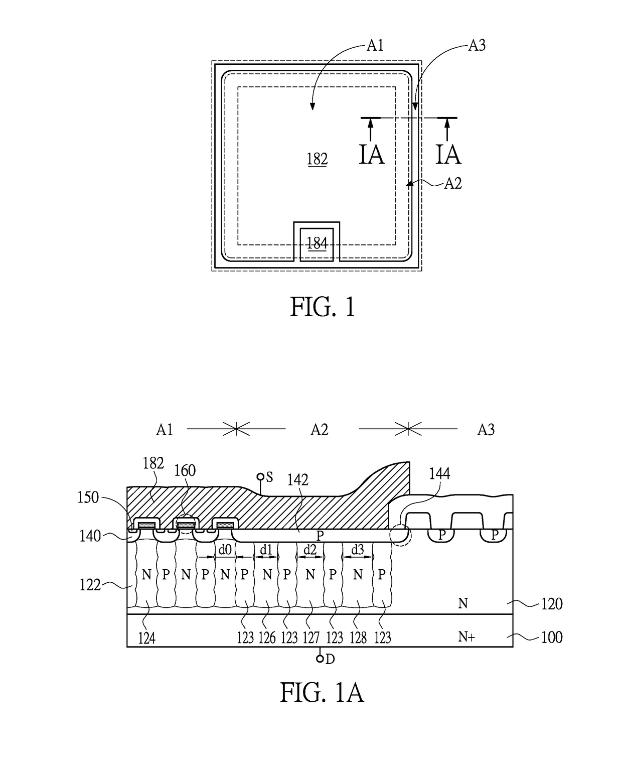
[0026]FIG. 1 and FIG. 1A are schematic views of a power MOS device in accordance with the present invention, wherein FIG. 1 is a top view of the power MOS device, and FIG. 1A is a cross-section view of the power MOS device along cross-section IA-IA of FIG. 1. As shown, the power MOS device, such as a MOSFET, is formed on a N-type heavily-doped semiconductor substrate 100 and includes an active area A1, a breakdown-first area A2, and a termination area A3. The breakdown-first area A2 is located between the active area A1 and the termination area A3. A P-type channel stopper 144 is located between the breakdown-first area A2 and the termination area A3 to prevent the generation of parasitic channel.

[0027]As shown, the active area A1 is located in the center of the power MOS device (such as a chip), the breakdown-first area A2 surrounds the active area A1, and the termination area A3 surrounds the breakdown-first area A2 and is located near the edge of the power MOS device. It is noted...

second embodiment

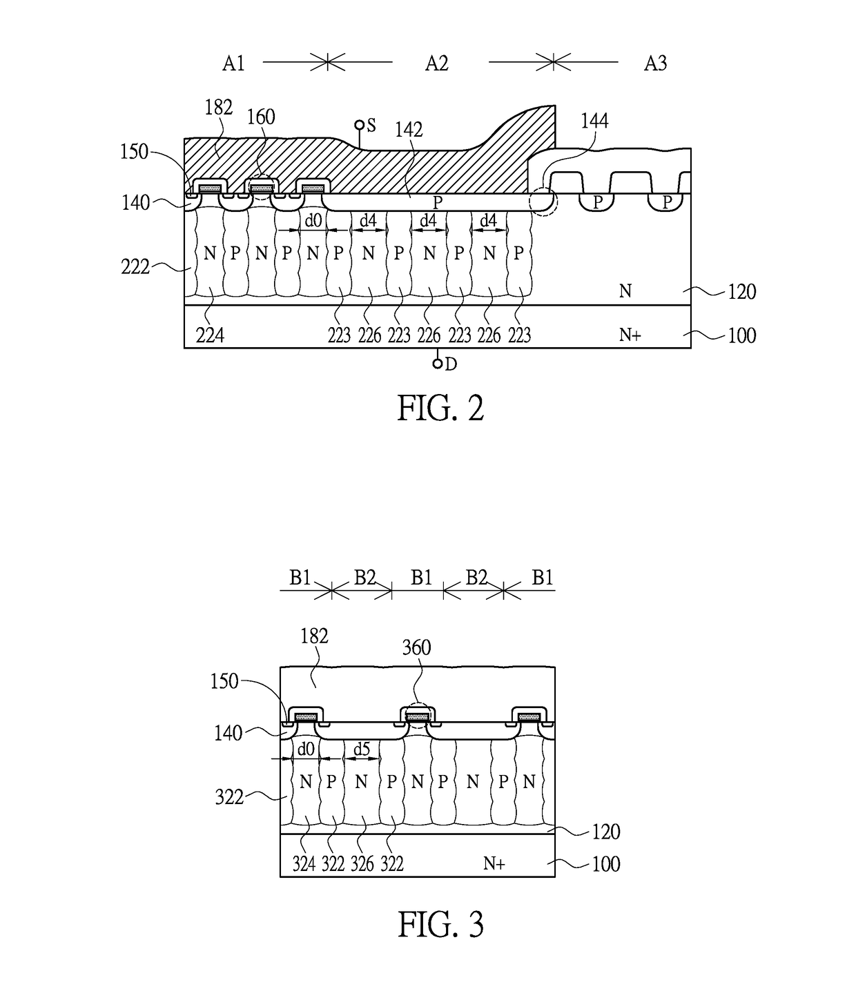
[0033]In the present embodiment, the intervals d1, d2, d3 of the neighboring breakdown-first P-type doping regions 123 (corresponding to the width of the breakdown-first N-type doping regions 126, 127, 128) are greater than the interval d0 of the neighboring active area P-type doping regions 122 to have BVDSS of the breakdown-first area A2 smaller than that of the active area A1. In addition, as a preferred embodiment of the present invention, the intervals d1, d2, d3 gradually increase along the direction from the active area A1 to the termination area A3 (i.e. d123). However, the present invention is not so restricted. As shown in FIG. 2, in the power MOS device of the present invention, the interval d4 of the breakdown-first P-type doping regions 223 (corresponding to the width of the breakdown-first N-type doping regions 226) is greater than the interval d0 of the neighboring active area P-type doping regions 122 but remains constant.

[0034]In the above mentioned embodiments, the...

third embodiment

[0037]FIG. 3 is a schematic view of the power MOS device in accordance with the present invention. As shown, in the present embodiment, an additional N-type doping region 326 is formed between two neighboring P-type doping regions 322 adjacent to two neighboring gate structures 360. Width d5 of the N-type doping region 326 is greater than width d0 of the N-type doping regions 324 right under the gate structures 360. The portion covered by the N-type doping region 326 and the two adjacent P-type doping regions 322 are regarded as the breakdown-first area B2. Thus, in the present embodiment, the breakdown-first area B2 of the power MOS device includes a lots of portions distributed in the active area B1 with a mesh structure. In detail, the active area B1 of the present embodiment is a net with a plurality of meshes, and the breakdown-first areas B2 are located in the meshes. As a preferred embodiment of the present invention, each of the portions of breakdown-first area B2 of the pre...


PUM


Abstract

A power metal-oxide-semiconductor (MOS) device is provided. The power MOS device is formed on a semiconductor substrate and includes an active region and a breakdown generated region. The active region includes a plurality of P-type doping regions and a plurality of N-type doping region alternatively arrayed between a source electrode and a drain electrode, and also includes a plurality of gate structures for controlling the conductive state of the active region. The breakdown generated region includes at least one P-type doping region and at least one N-type doping region alternatively arrayed between a source electrode and a drain electrode, and the breakdown voltage of the breakdown generated region is smaller than that of the active region.

Description

BACKGROUND OF THE INVENTION[0001]1. Field of the Invention[0002]The present invention is related to a power metal-oxide-semiconductor (MOS) device, and more particularly related to a power MOS device with super junction structure featuring low on resistance.[0003]2. Description of Related Art[0004]Super-junction MOS device is a power semiconductor device suitable for high frequency and high voltage applications, and is broadly used in various categories with the needs of high electric density, or high system efficiency and reliability.[0005]The super junction MOS device includes a plurality of P-type pylons located in a N-type epitaxial layer extending along the depth direction of the N-type epitaxial layer. The P-type pylons are in parallel with each other and spaced apart with a predetermined interval. A plurality of gate structures is formed above the N-type epitaxial layer for controlling the conductive states of the channel between the source electrode above the epitaxial layer...

Claims


Application Information

Patent Timeline
Patent Type & Authority Applications(United States)
IPC IPC(8): H01L29/06H01L29/78
CPCH01L29/0634H01L29/78H01L29/0688H01L29/0615H01L29/0619H01L29/66712H01L29/7811
Inventor TU, KAO-WAYCHANG, YUAN-SHUNHSU, TZU-HSU
Owner BRIGHT TOWARD IND CO LTD
Why Eureka
Try Eureka