Semiconductor structure

a technology of semiconductors and structures, applied in the field of semiconductor structures, can solve problems such as high driving voltage, and achieve the effect of preventing a rise in driving voltage and increasing the efficiency of electron impedance performan

Inactive Publication Date: 2017-09-14
GENESIS PHOTONICS
View PDF9 Cites 5 Cited by
  • Summary
  • Abstract
  • Description
  • Claims
  • Application Information

AI Technical Summary

Benefits of technology

[0006]The disclosure provides a semiconductor structure having a hole supply layer, in which an electron impedance performance is increased by adjusting an aluminum content in the hole supply layer, thereby preventing a rise in driving voltage.

Problems solved by technology

However, although the aluminum indium gallium nitride having the high aluminum content can effectively enhance an electron impedance effect, it is accompanied by the issue of high driving voltage.

Method used


Image

  • Semiconductor structure
  • Semiconductor structure
  • Semiconductor structure

Examples


Embodiment Construction

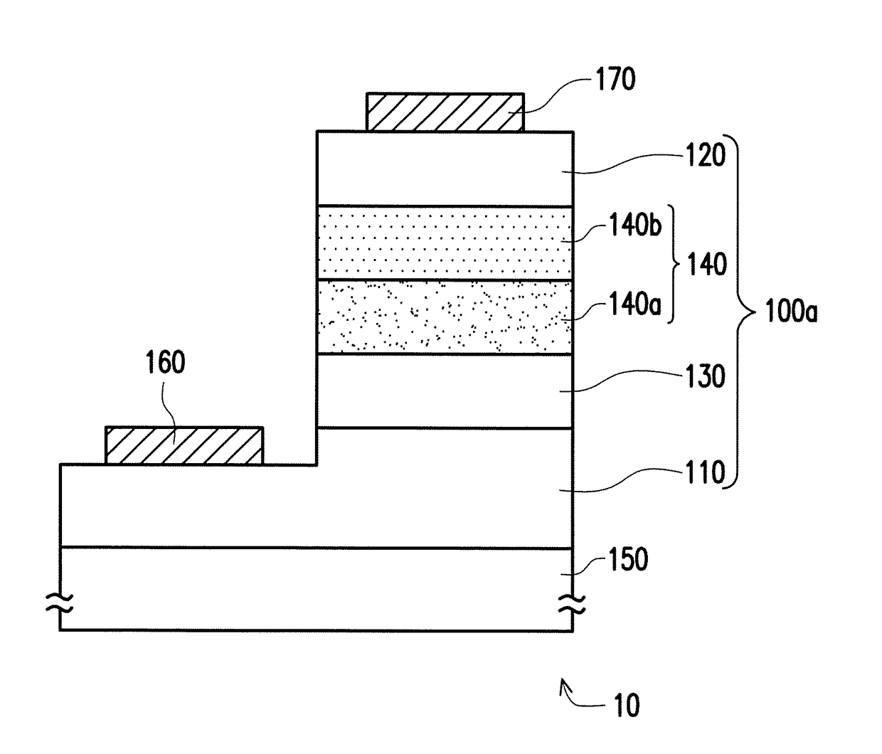
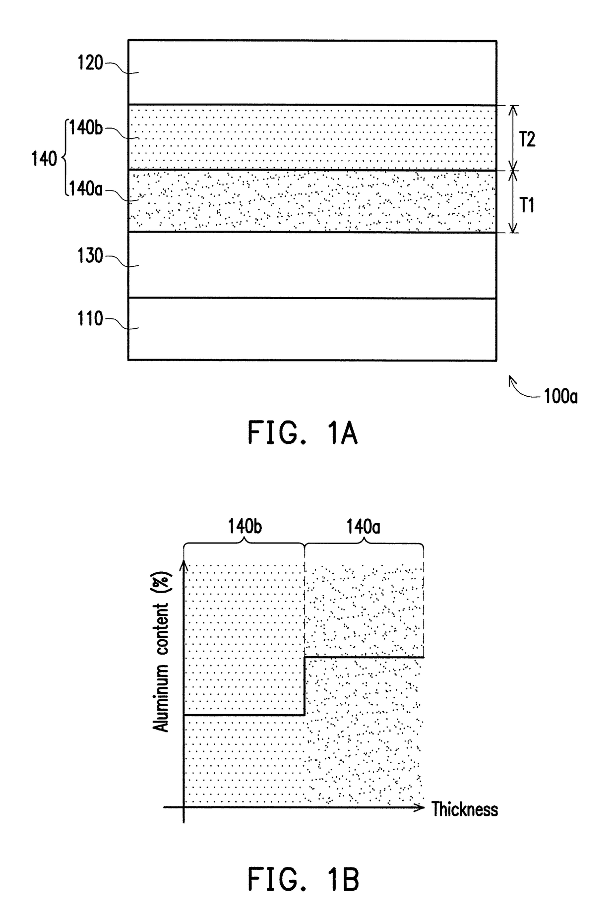
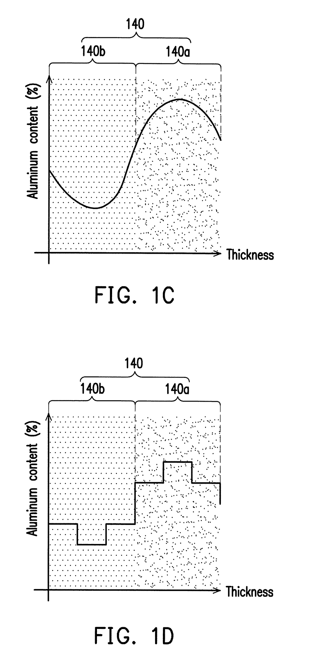
[0047]FIG. 1A is a schematic cross-sectional diagram illustrating a semiconductor structure according to an embodiment of the disclosure. Referring to FIG. 1A, in the present embodiment, a semiconductor structure 100a includes a first-type semiconductor layer 110, a second-type semiconductor layer 120, a light emitting layer 130 and a hole supply layer 140. The light emitting layer 130 is disposed between the first-type semiconductor layer 110 and the second-type semiconductor layer 120. The hole supply layer 140 disposed between the light emitting layer 130 and the second-type semiconductor layer 120, and the hole supply layer 140 includes a first hole supply layer 140a and a second hole supply layer 140b. The first hole supply layer 140a is disposed between the light emitting layer 130 and the second hole supply layer 140b, and a chemical formula of the first hole supply layer 140a is Alx1Iny1Ga1-x1-y1N, wherein 0≦x1140b is disposed between the first hole supply layer 140a and the...


PUM


Abstract

A semiconductor structure includes a first-type semiconductor layer, a second-type semiconductor layer, a light emitting layer and a hole supply layer. The light emitting layer is disposed between the first-type semiconductor layer and the second-type semiconductor layer. The hole supply layer is disposed between the light emitting layer and the second-type semiconductor layer, and the hole supply layer includes a first hole supply layer and a second hole supply layer. The first hole supply layer is disposed between the light emitting layer and the second hole supply layer, and a chemical formula of the first hole supply layer is Alx1Iny1Ga1-x1-y1N, wherein 0≦x1<0.4, and 0≦y1<0.4. The second hole supply layer is disposed between the first hole supply layer and the second-type semiconductor layer, a chemical formula of the second hole supply layer is Alx2Iny2Ga1-x2-y2N, wherein 0≦x2<0.4, 0≦y2<0.4, and x1>x2.

Description

CROSS-REFERENCE TO RELATED APPLICATION[0001]This application claims the priority benefit of Taiwan application serial no. 105106975, filed on Mar. 8, 2016. The entirety of the above-mentioned patent application is hereby incorporated by reference herein and made a part of this specification.BACKGROUND OF THE INVENTION[0002]1. Field of the Invention[0003]The present disclosure generally relates to a semiconductor structure, and more particularly, to a semiconductor structure having a hole supply layer.[0004]2. Description of Related Art[0005]In a conventional light-emitting diode chip, in order to increase the possibility for combining electrons and holes and to elevate the electron impedance, a quaternary aluminum indium gallium nitride (AlxInyGa1-x-yN) semiconductor layer having a high aluminum content is disposed between a light emitting layer and a P-type semiconductor layer, and this semiconductor layer may be doped with a high concentration of magnesium or carbon. However, alth...

Claims


Application Information

Patent Timeline
Patent Type & Authority Applications(United States)
IPC IPC(8): H01L33/14H01L33/06H01L33/32
CPCH01L33/14H01L33/06H01L33/325H01L33/32H01L33/025H01L33/02
Inventor LIN, CHENG-HUNGHUANG, JENG-JIEHUANG, CHI-FENG
Owner GENESIS PHOTONICS
Why Eureka
Try Eureka