Method for fabricating photoresist pattern, color filter and display device

a display device and photoresist pattern technology, applied in the field of display technology, can solve the problems that the black matrix having a line width of around 5 m cannot meet the requirements of lcd products in terms of the job is highly demanding, so as to improve the transmittance ratio and aperture ratio of the display device

Inactive Publication Date: 2017-09-21
CHENGDU BOE OPTOELECTRONICS TECH CO LTD +1
View PDF5 Cites 10 Cited by
  • Summary
  • Abstract
  • Description
  • Claims
  • Application Information

AI Technical Summary

Benefits of technology

[0006]The present disclosure provides in some embodiments a method for fabricating a photoresist pattern, a color filter and a method for fabricating the same, and a display device, which can achieve a black matrix having a narrow line width and improve its transmittance ratio and aperture ratio of the display device.
[0025]According to the method for fabricating the photoresist pattern, the color filter and the method for fabricating the same, and the display device provided by embodiments of the present disclosure, negative photoresist and positive photoresist are coated on a base substrate to form a first photoresist layer and a second photoresist layer at first. Further, a first exposure process and a first developing process are conducted on first regions of the second photoresist layer, so as to remove the positive photoresist within the first regions of the second photoresist layer and the negative photoresist within second regions of the first photoresist layer, and to obtain a first photoresist pattern retained within the second photoresist layer and a second photoresist pattern retained within the first photoresist layer, wherein a line width of the first photoresist pattern is larger than that of the second photoresist pattern, and a projection of each of the first regions on the base substrate is located within that of a corresponding one of the second regions on the base substrate. Finally, a second exposure process is conducted on the first photoresist pattern and the second photoresist pattern, and a second developing process is conducted to remove the first photoresist pattern but to retain the second photoresist pattern that serves as the black matrix. As seen from the above, as for the first developing process, the first regions of the second photoresist layer exposed react with the developer and dissolve. After the dissolve process completes, the negative photoresist within the first photoresist layer that has not yet been exposed and is beneath the first regions happens to dissolve in turn. Further, the negative photoresist that is covered by the unexposed second photoresist layer happens to dissolve alike, due to its contact with the developer in a lateral direction, which results in that peripheral parts of the negative photoresist that is covered by the unexposed second photoresist layer dissolves. As a result, by taking advantage of the positive photoresist within the second photoresist layer as a surface cover, the negative photoresist within the first photoresist layer is prevented from getting a direct and large-area contact with developer for reaction. As such, when the negative photoresist is adopted as the black negative photoresist used for fabricating the black matrix, a film / layer peel-off occurrence due to a direct contact between black matrix photoresist and developer for fabricating the black matrix having a narrow line width can be prevented, the black matrix having a narrow line width can be achieved accordingly, and its transmittance ratio and aperture ratio of the display device can be improved.

Problems solved by technology

Nevertheless, as products having high Pixels Per Inch (PPI) are prevailing in the market, a black matrix having a line width of around 5 μm can hardly meet the requirements for LCD products in terms of transmittance ratio and aperture ratio.
Therefore, it is a highly demanding job to come up with a solution about how to fabricate a black matrix pattern having a narrow line width.

Method used


Image

  • Method for fabricating photoresist pattern, color filter and display device
  • Method for fabricating photoresist pattern, color filter and display device
  • Method for fabricating photoresist pattern, color filter and display device

Examples


Embodiment Construction

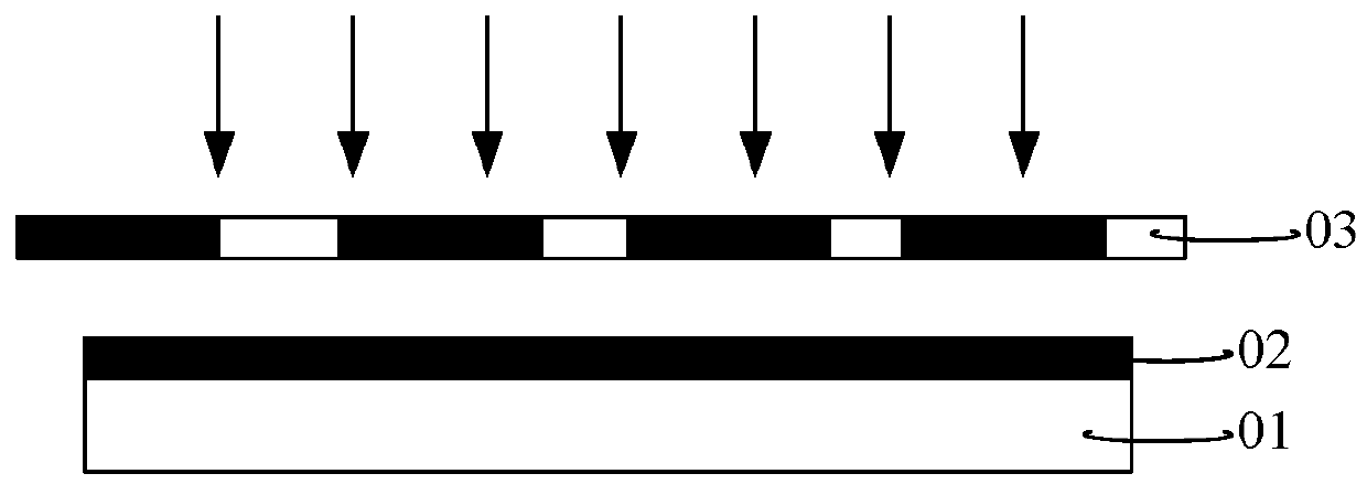
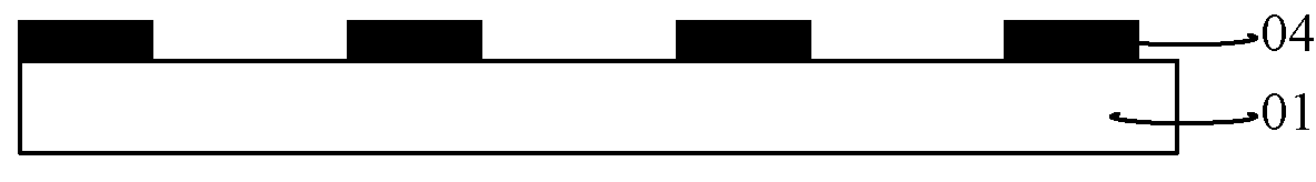
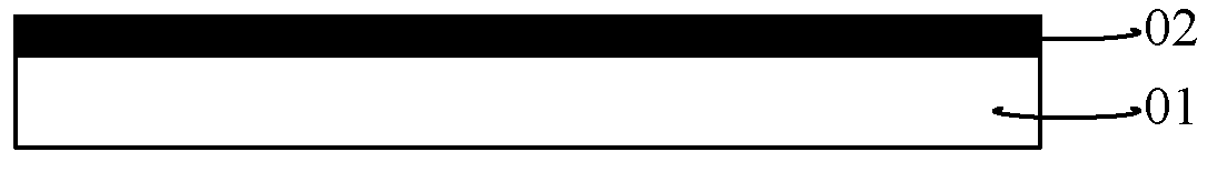
[0040]With respect to the following description, not for the purpose of limitation but for the purpose of description, detailed description about particular system structures, interfaces, and techniques has been given for better appreciation of the present disclosure. However, a skilled person can understand that the present disclosure can also be achieved without certain detailed description in some embodiments. In other cases, detailed description on well-known devices, circuits, and methods has been omitted, so as not to obscure the essence of the present disclosure unnecessarily.

[0041]Unless otherwise defined, any technical or scientific terms used herein shall have the common meaning understood by a person of ordinary skills. Such words as “first” and “second” used in the specification and claims are merely used to differentiate different components rather than to represent any order, number or importance. Unless otherwise indicated, “a plurality of” refers to two or more than ...


PUM

PropertyMeasurementUnit
widthaaaaaaaaaa
widthaaaaaaaaaa
widthaaaaaaaaaa

Abstract

The disclosure provides in some embodiments a method for fabricating a photoresist pattern, a color filter and a method for fabricating the same, and a display device. The method for fabricating a photoresist pattern includes coating negative photoresist on a base substrate to form a first photoresist layer, coating positive photoresist on the first photoresist layer to form a second photoresist layer, conducting a first exposure process on first regions of the second photoresist layer, conducting a first developing process to remove the positive photoresist within the first regions of the second photoresist layer and the negative photoresist within second regions of the first photoresist layer, so as to obtain a first photoresist pattern and a second photoresist pattern, conducting a second exposure process on the first photoresist pattern and the second photoresist pattern, and conducting a second developing process to remove the first photoresist pattern.

Description

CROSS-REFERENCE TO RELATED APPLICATION[0001]This application claims priority of Chinese Patent Application No. 201510617500.4, which was filed on Sep. 24, 2015, the disclosures of which are incorporated herein by reference in their entirety.FIELD[0002]This disclosure relates to the field of displaying technology, in particular to a method for fabricating a photoresist pattern, a color filter, and a display device.BACKGROUND[0003]A color filter is one of key elements for colorization of a Liquid Crystal Display (LCD). Specifically, through the color filter, strong light rays emitted by a backlight module of the LCD can be converted into a colorful picture. With respect to fabricating a color filter, a black matrix is to be disposed on a glass substrate in form of grids, and then color blocking elements for three primary colors, i.e., Red (R), Green (G), and Blue (B), are arranged on respective pixel units defined by the black matrix in turn.[0004]As shown in FIG. 1, when fabricating ...

Claims


Application Information

Patent Timeline
Patent Type & Authority Applications(United States)
IPC IPC(8): G02F1/1335G03F7/00G02B5/20
CPCG02F1/133512G02B5/201G02F2001/133519G03F7/0007G02F1/133516G03F7/105G03F7/2022G03F7/322G03F7/095G03F7/2024G02F1/133519G03F7/0955G03F7/2032
Inventor LONG, QINGDEKANG, YULONGLIANG, YUANZHANG, ZHIYONGFAN, LIWEI
Owner CHENGDU BOE OPTOELECTRONICS TECH CO LTD
Why Eureka
Try Eureka