Manufacturing method of circuit board and stamp

a manufacturing method and circuit board technology, applied in the field of circuit board and stamp manufacturing method, can solve the problems of poor process yield, easy damage of photoresist pattern to be formed, and inability to remove residual photoresist layer in a simple manner, and achieve the effect of easy removal

Active Publication Date: 2017-09-21
UNIMICRON TECH CORP
View PDF1 Cites 0 Cited by
  • Summary
  • Abstract
  • Description
  • Claims
  • Application Information

AI Technical Summary

Benefits of technology

[0018]Based on the above, in the invention, since the pressing side of the stamp becomes sticky when subjected to pressure in the imprinting process, in the forming process of the patterned photoresist layer or the p

Problems solved by technology

However, after NIL transfers a pattern to a photoresist material, comprehensive exposure needs to be performed, and therefore the patterned photoresist layer to be formed and unnecessary residual photoresist material are both exposed to light.
As a result, the residual photoresist layer cannot be removed by a developing solution in a simple manner.
Therefore, unnecessary pho

Method used


Image

  • Manufacturing method of circuit board and stamp
  • Manufacturing method of circuit board and stamp
  • Manufacturing method of circuit board and stamp

Examples


first embodiment

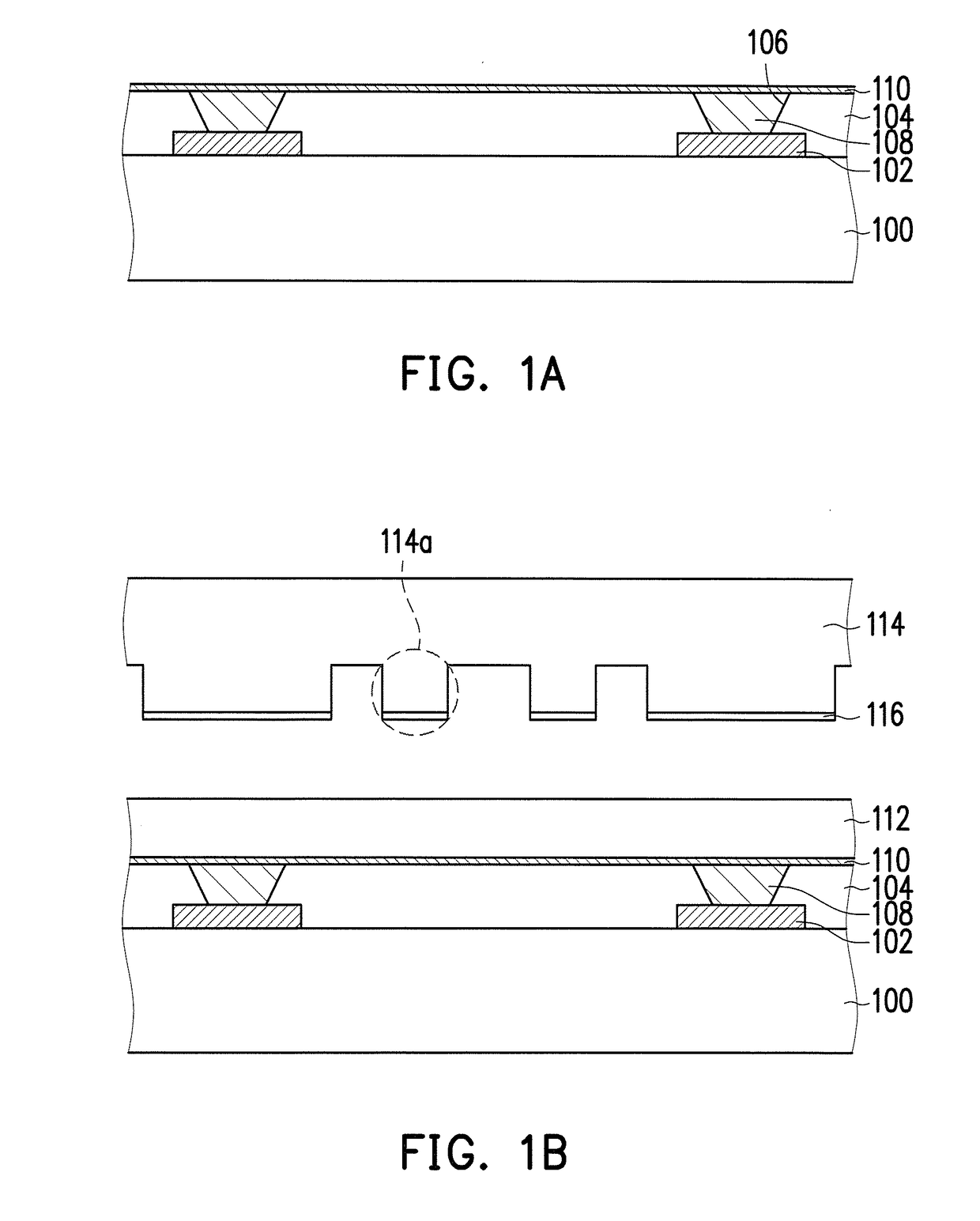
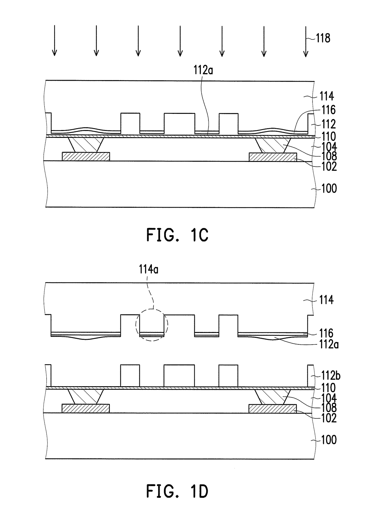
[0024]FIG. 1A to FIG. 1F are cross-sectional schematics of the manufacturing process of a circuit board shown according to the first embodiment of the invention. First, referring to FIG. 1A, a circuit pattern 102 is formed on a dielectric substrate 100. The forming method of the circuit pattern 102 includes, for instance, forming a conductive layer on the dielectric substrate 100 via a lamination method on the conductive layer and performing a patterning process. The material of the dielectric substrate 100 is, for instance, epoxy resin, glass fiber cloth, or ceramic. The material of the conductive layer is, for instance, copper. Next, a dielectric layer 104 is formed on the dielectric substrate 100. The dielectric layer 104 covers the circuit pattern 102 on the dielectric substrate 100. The material of the dielectric layer 104 is, for instance, epoxy resin. The dielectric layer 104 is, for instance, formed on the dielectric substrate 100 via a lamination method. Next, a hole 106 ex...

second embodiment

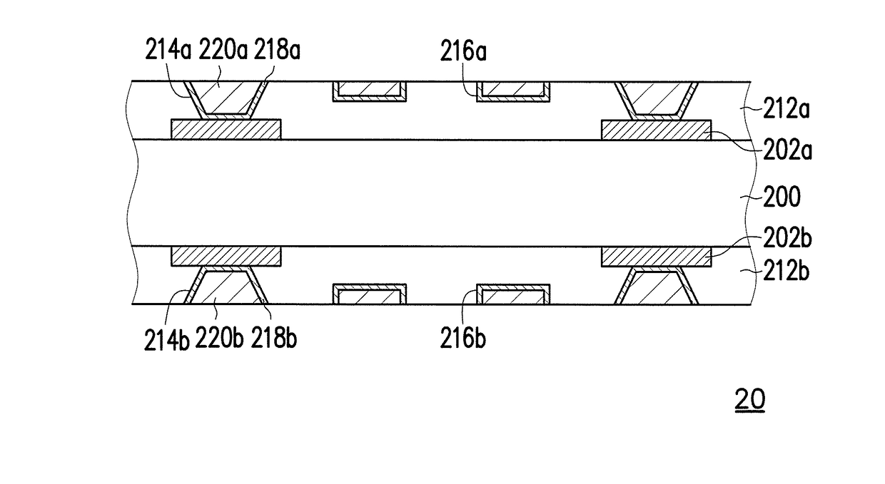
[0034]FIG. 2A to FIG. 2D are cross-sectional schematics of the manufacturing process of a circuit board shown according to the second embodiment of the invention. First, referring to FIG. 2A, a circuit pattern 202a is formed on a first surface 200a of a dielectric substrate 200, and a circuit pattern 202b is formed on a second surface 200b of the dielectric substrate 200. The forming method of the circuit patterns 202a and 202b includes, for instance, forming a conductive layer respectively on the first surface 200a and the second surface 200b via a lamination method and performing a patterning process on the conductive layer. The material of the dielectric substrate 200 is, for instance, epoxy resin, glass fiber cloth, or ceramic. The material of the conductive layer is, for instance, copper. Then, a dielectric layer 204a is formed on the first surface 200a and a dielectric layer 204b is formed on the second surface 200b. The dielectric layer 204a covers the circuit pattern 202a on...


PUM

PropertyMeasurementUnit
Pressureaaaaaaaaaa
Photosensitivityaaaaaaaaaa

Abstract

A manufacturing method of a circuit board and a stamp are provided. The method includes the following steps. A circuit pattern and a dielectric layer covering the circuit pattern are formed on a dielectric substrate. A conductive via connected to the circuit pattern is formed in the dielectric layer. A photoresist material layer is formed on the dielectric layer. An imprinting process is performed on the photoresist material layer using a stamp to form a patterned photoresist layer, wherein the pressing side of the stamp facing the circuit pattern becomes sticky when subjected to pressure so as to catch photoresist residue from the photoresist material layer in the imprinting process. A patterned metal layer is formed on a region exposed by the patterned photoresist layer. The patterned photoresist layer is removed.

Description

CROSS-REFERENCE TO RELATED APPLICATION[0001]This application claims the priority benefit of U.S. provisional application Ser. No. 62 / 309,930, filed on Mar. 17, 2016. The entirety of the above-mentioned patent application is hereby incorporated by reference herein and made a part of this specification.BACKGROUND OF THE INVENTION[0002]Field of the Invention[0003]The invention relates to a manufacturing method of a circuit board and a stamp, and more particularly, to a manufacturing method of a circuit board in which photoresist residue or dielectric residue is removed using an adhesive layer and a stamp used in the method.[0004]Description of Related Art[0005]Nano-imprint lithography (NIL) is a technique for manufacturing fine circuits and is extensively applied in the LED and OLED industries. NIL includes pressing a mold prototype having a pattern (generally referred to as mold, stamp, or template) on a photoresist material to mechanically deform the mold prototype so as to precisely...

Claims


Application Information

Patent Timeline
IPC IPC(8): H05K3/06G03F7/16G03F7/20H05K1/11
CPCH05K3/064H05K1/115H05K3/06H05K2203/0548G03F7/20H05K2201/091G03F7/162G03F7/0002H05K3/465Y10T29/49124Y10T29/49155H05K3/108H05K3/4644H05K2203/0108Y10T29/5313H05K3/0023H05K2203/0369H05K2203/0562H05K2203/0502
Inventor CHENG, SHIH-LIAN
Owner UNIMICRON TECH CORP
Why Eureka
Try Eureka