Monolithic 3-d dynamic memory and method

a dynamic memory and monolithic technology, applied in semiconductor devices, digital storage, instruments, etc., can solve the problems of limited endurance in memory cells, easy to disturb the stored charge contents of each cell, and easy to read-pass voltages, so as to achieve enhanced program and erase endurance levels, the effect of reducing p/e voltages and smallest footprin

Inactive Publication Date: 2017-09-28
SCHILTRON
View PDF0 Cites 102 Cited by
  • Summary
  • Abstract
  • Description
  • Claims
  • Application Information

AI Technical Summary

Benefits of technology

[0015]One advantage of the present invention is enhanced program and erase (P / E) endurance levels, while operating with reduced P / E voltages. Because dual-gate devices are used, the memory cells of the present invention—which are configured as strings in a memory structure of the smallest footprint—may be read or programmed while minimizing the disturbs on the memory cells connecting up to the one being read or programmed.
[0016]The present invention is better understood upon consideration of the detailed description below in conjunction with the accompanying drawings.

Problems solved by technology

One of the main challenges in DRAM cell design at that feature size is keeping the capacitance of the cell capacitor large enough to be sensed.
However, the reduced damage is achieved at the expense of retention, since the stored charge will leak away.
However, the higher programming and erase voltages result in a limited endurance in the memory cells.
Since each device in the string can be programmed or erased at a low voltage, the “read-pass” voltages can easily disturb the stored charge contents of each cell.

Method used


Image

  • Monolithic 3-d dynamic memory and method
  • Monolithic 3-d dynamic memory and method
  • Monolithic 3-d dynamic memory and method

Examples


Embodiment Construction

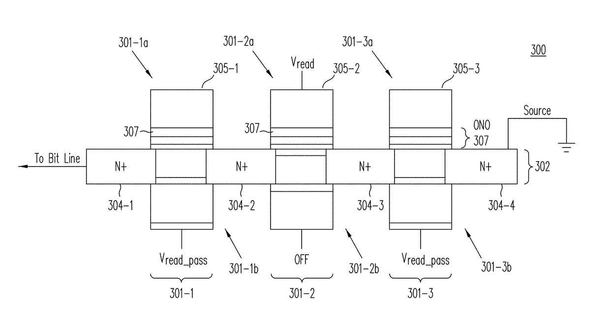
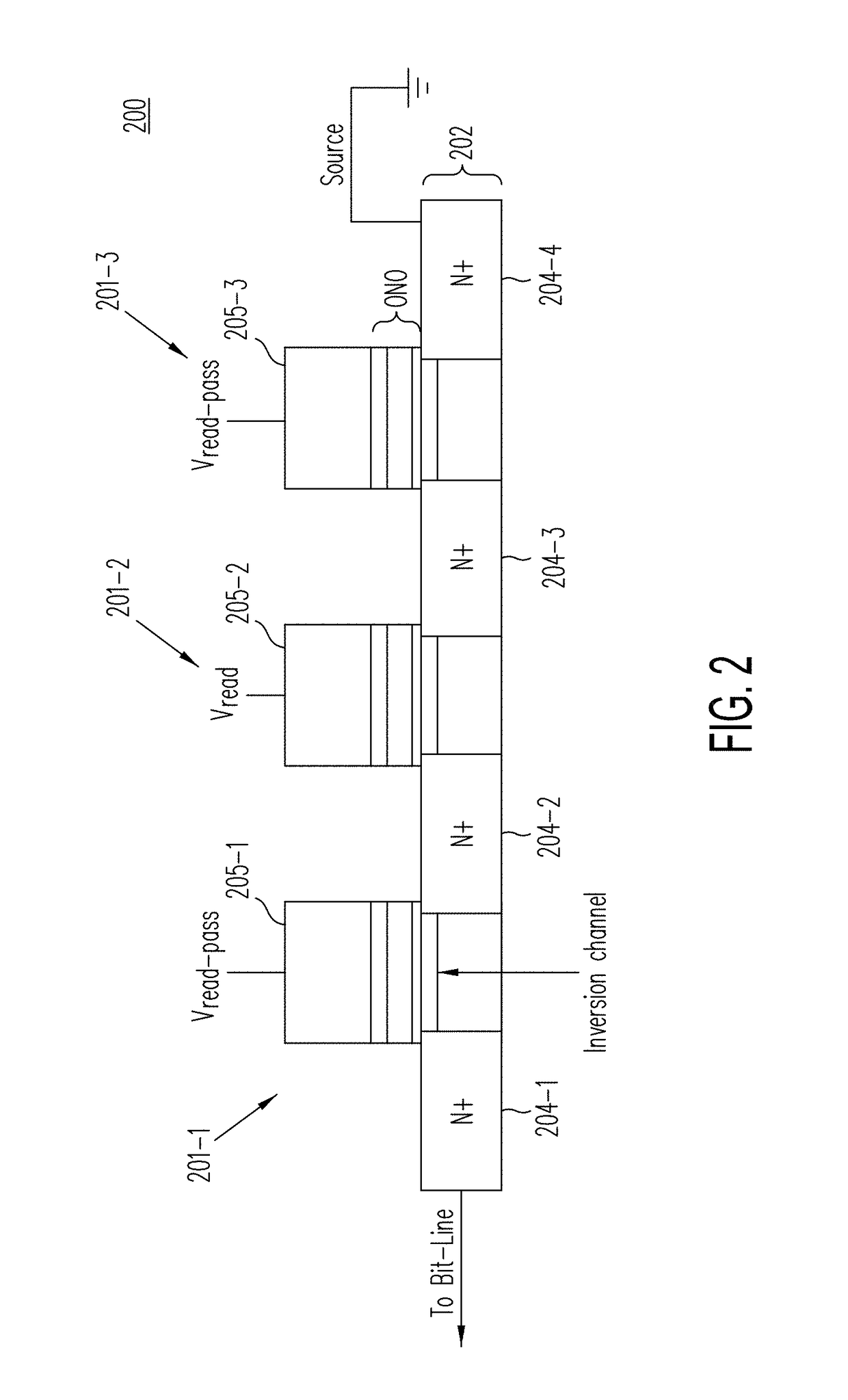
[0021]The present invention provides a memory cell and a method that overcome the difficulties of the prior art. FIG. 3 shows dual-gate contactless string (“NAND string”) 300 including dual-gate devices 301-1, . . . , 301-n (n=3, for illustratively purpose only), in accordance with one embodiment of the present invention. As shown in FIG. 3, dual-gate transistors 301-1, . . . , 301-n are formed in conjunction with a silicon substrate, referred herein as thin-film layer 302. Active devices (e.g., 301-2a and 301-2b) are formed one on each side of thin film layer 302, between a pair of drain or source regions (e.g., 304-2 and 304-3). In FIG. 3, charge storage layer 307, typically an oxide-nitride-oxide (ONO) layer is provided in one of the active devices (“storage devices,” e.g., active devices 301-1a. 301-2a and 301-3a) on the side of thin-film layer 302 opposite that of the access devices. Active devices formed on the other side of substrate or thin-film layer 302 (e.g., active devic...


PUM


Abstract

A monolithic 3-D dynamic memory structure includes independently addressable strings of dual-gate devices. In each dual-gate device charge is deliberately stored on one side of the dual-gate. Although the stored charge may leak away, the stored charge in a dual-gate device of the present invention need only be refreshed at much longer intervals than conventional DRAM cells.

Description

CROSS REFERENCE TO RELATED APPLICATIONS[0001]The present application relates to and claims priority of U.S. provisional patent application (“Provisional Application”), Ser. No. 62 / 311,802, entitled “Monolithic 3-D Dynamic Memory and Method,” filed Mar. 22, 2016. The disclosure of the Provisional Application is hereby incorporated by reference in its entirety.BACKGROUND OF THE INVENTION[0002]1. Field of the Invention[0003]The present invention relates to semiconductor structures for implementing memory circuits. In particular, the present invention relates to a 3-dimensional semiconductor structure for implementing a dynamic memory cell.[0004]2. Description of the Related Art[0005]Scaling of dynamic random access memory (DRAM) circuits is expected to reach a limit at close to 20 nm minimum feature size. (See, e.g., the article, entitled “Technology scaling challenge and future prospects of DRAM and NAND flash memory” by S.-K. Park, published in IEEE International Memory Workshop (IMW...

Claims


Application Information

Patent Timeline
Patent Type & Authority Applications(United States)
IPC IPC(8): H01L27/11578G11C11/22H01L27/11597H01L27/1159H01L27/1157H01L27/11573
CPCH01L27/11578H01L27/1157H01L27/11573G11C16/32H01L27/1159G11C11/223G11C16/08H01L27/11597H01L28/00G11C16/0483G11C11/406G11C2211/4016H10B43/20H10B43/35H10B43/40H10B51/20H10B51/30
Inventor WALKER, ANDREW J.HARARI, ELI
Owner SCHILTRON
Why Eureka
Try Eureka