Thin film transistor array panel and method of manufacturing the same

a technology of thin film transistors and array panels, which is applied in the direction of transistors, electrical devices, semiconductor devices, etc., can solve the problems of relative low charge mobility, relatively high manufacturing cost, and the development of problems involving amorphous silicon in manufacturing high-performance thin film transistors, so as to prevent (or reduce) the deterioration of mechanical and viewing characteristics

Active Publication Date: 2017-09-28
SAMSUNG DISPLAY CO LTD
View PDF3 Cites 3 Cited by
  • Summary
  • Abstract
  • Description
  • Claims
  • Application Information

AI Technical Summary

Benefits of technology

[0008]One or more exemplary embodiments provide a thin film transistor array panel configur

Problems solved by technology

Amorphous silicon provides relatively low charge mobility and allows for a relatively simple manufacturing process, but issues may develop with respect to utilizing amorphous silicon in manufacturing high-performance thin film transi

Method used


Image

  • Thin film transistor array panel and method of manufacturing the same
  • Thin film transistor array panel and method of manufacturing the same
  • Thin film transistor array panel and method of manufacturing the same

Examples


Embodiment Construction

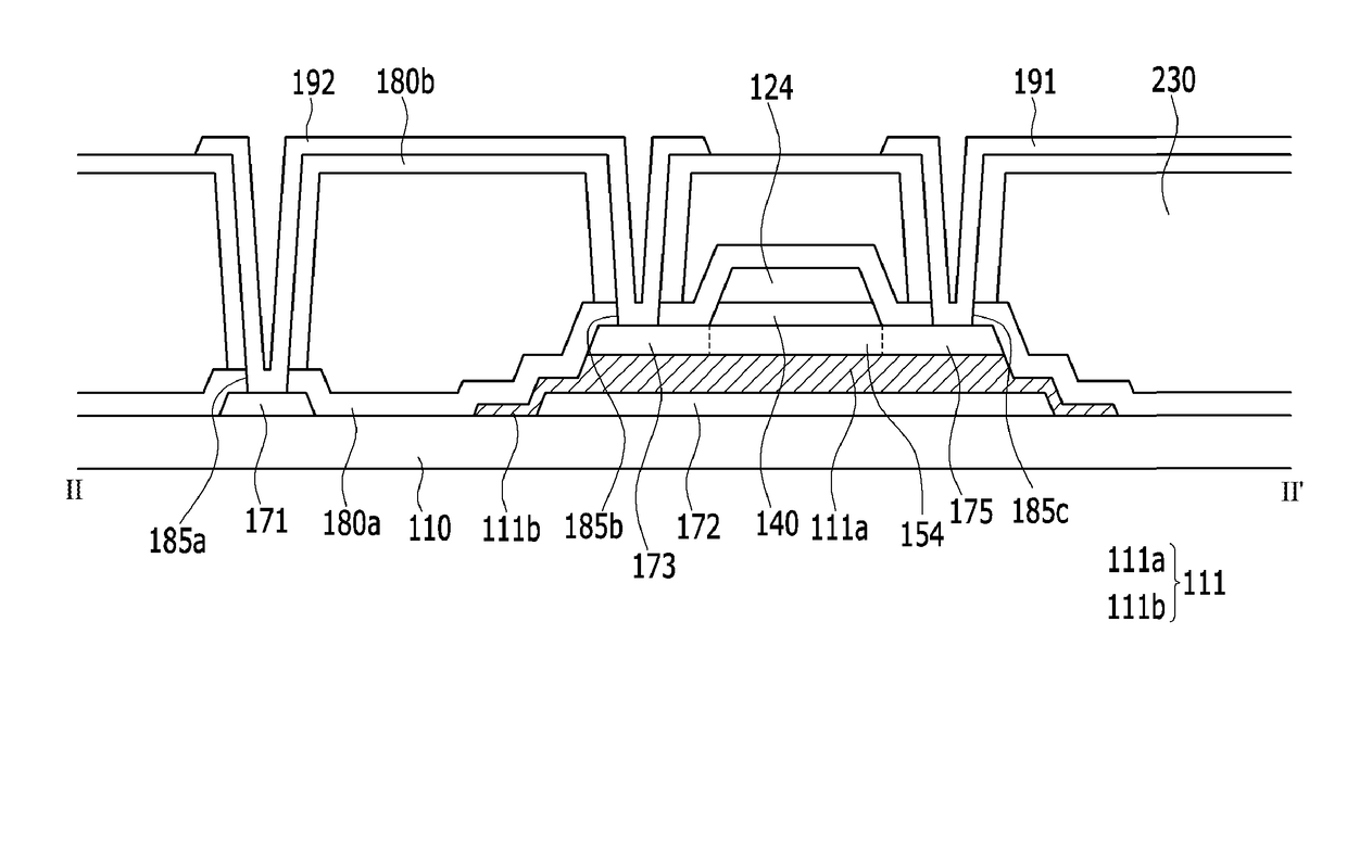
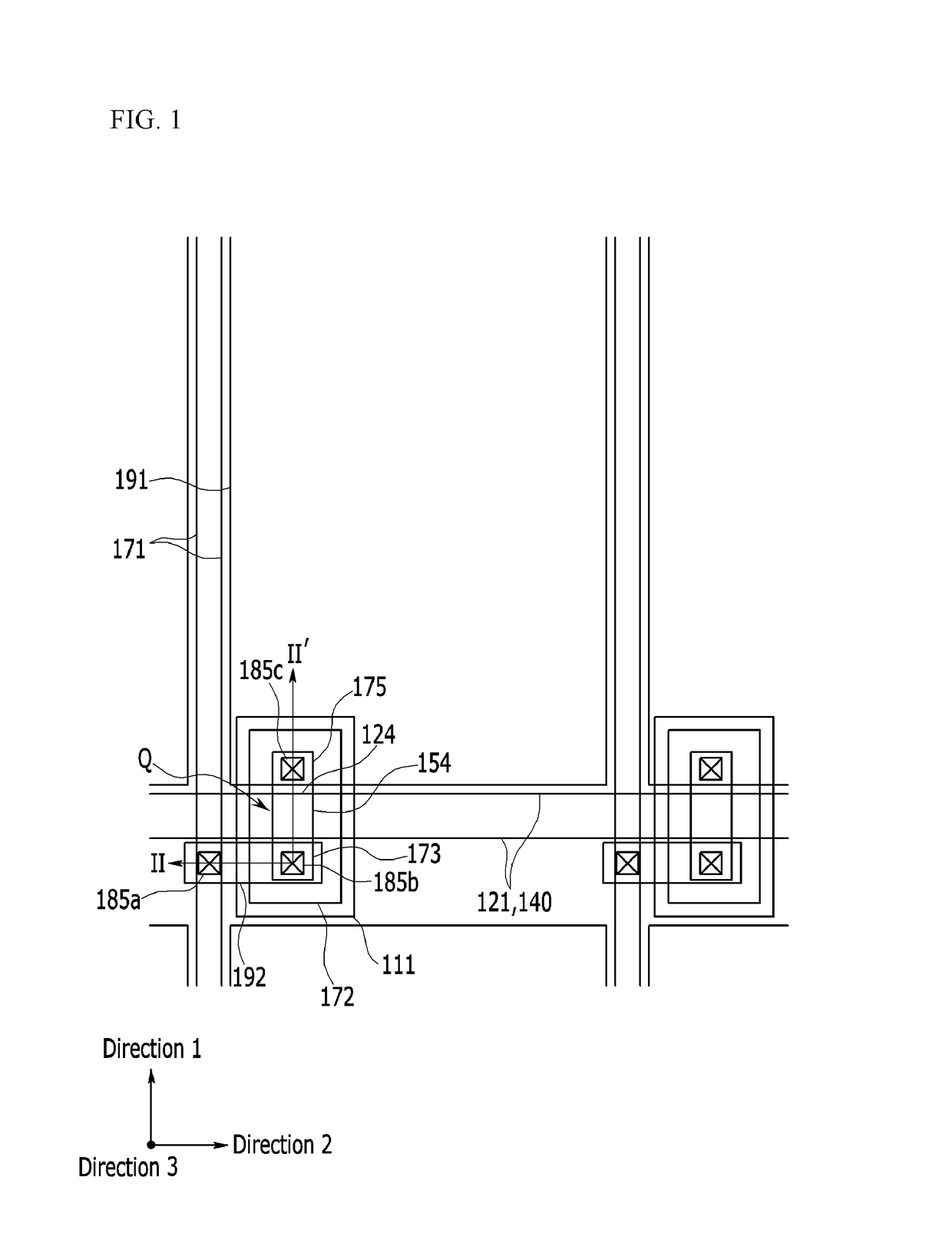
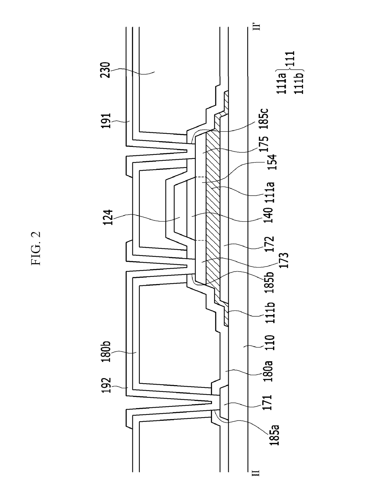
[0028]In the following description, for the purposes of explanation, numerous specific details are set forth in order to provide a thorough understanding of various exemplary embodiments. It is apparent, however, that various exemplary embodiments may be practiced without these specific details or with one or more equivalent arrangements. In other instances, well-known structures and devices are shown in block diagram form in order to avoid unnecessarily obscuring various exemplary embodiments.

[0029]Unless otherwise specified, the illustrated exemplary embodiments are to be understood as providing exemplary features of varying detail of various exemplary embodiments. Therefore, unless otherwise specified, the features, components, modules, layers, films, panels, regions, and / or aspects of the various illustrations may be otherwise combined, separated, interchanged, and / or rearranged without departing from the disclosed exemplary embodiments. Further, in the accompanying figures, the...


PUM


Abstract

A thin film transistor array panel includes a substrate; a data line disposed on the substrate; a buffer layer disposed on the substrate and spaced apart from the data line in a plan view; a thin film transistor disposed on the buffer layer, the thin film transistor including an oxide semiconductor layer; and a pixel electrode connected to the thin film transistor.

Description

CROSS-REFERENCE TO RELATED APPLICATION[0001]This application claims priority from and the benefit of Korean Patent Application No. 10-2016-0035386, filed on Mar. 24, 2016, which is hereby incorporated by reference for all purposes as if fully set forth herein.BACKGROUND[0002]Field[0003]The present disclosure relates to a thin film transistor array panel and a method of manufacturing the same.[0004]Discussion of the Background[0005]A thin film transistor (TFT) is used in various kinds of electronic devices, such as, for example, a display device. Thin film transistors may be used as switching element or driving elements in a liquid crystal display (LCD), an organic light emitting diode (OLED) display, and the like. Typically, a thin film transistor includes a gate electrode, a source electrode, a drain electrode facing the source electrode, and a semiconductor electrically connected to the source electrode and the drain electrode. Characteristics of the semiconductor generally determ...

Claims


Application Information

Patent Timeline
IPC IPC(8): H01L29/786H01L27/12
CPCH01L29/78606H01L27/1225H01L27/124H01L27/1288H01L29/78633H01L29/78696H01L29/7869H10K59/123H10K59/1213H01L29/78603H01L27/1218H01L29/78618H10K59/124H10K59/126H10K59/131
Inventor JEONG, YU-GWANGCHO, HYUN MINBAE, SU BINCHOI, SHIN IL
Owner SAMSUNG DISPLAY CO LTD
Why Eureka
Try Eureka