Method of Producing Multi-Layer Ceramic Electronic Component and Multi-Layer Ceramic Electronic Component

a technology of electronic components and ceramics, applied in the direction of fixed capacitors, stacked capacitors, fixed capacitor details, etc., can solve the problems of affecting the miniaturization, difficult to control the thickness of the side margins to be uniform, and difficult to provide ceramic paste in uniform thickness on the side surfaces of multi-layer chips, etc., to achieve easy deformation, enhance the release properties of ceramic paste, and enhance productivity

Inactive Publication Date: 2017-10-05
TAIYO YUDEN KK
View PDF6 Cites 8 Cited by
  • Summary
  • Abstract
  • Description
  • Claims
  • Application Information

AI Technical Summary

Benefits of technology

[0009]With this configuration, even when the ceramic paste immediately after being applied has a non-uniform thickness due to surface tension or the like, planarization of the ceramic paste can provide a uniform thickness. This can prevent the side margin from partially protruding, bulging, or the like, and provide the miniaturization of the multi-layer ceramic electronic component. Further, even when the ceramic paste immediately after being applied is thin at the circumference, the ceramic paste is pressed to flow to the circumference by planarization, so that the thickness of the circumferential portion can be sufficiently ensured. Therefore, insulation properties of the internal electrodes can be ensured.
[0026]As described above, according to the present invention, it is possible to provide a method of producing a multi-layer ceramic electronic component and a multi-layer ceramic electronic component, which are capable of sufficiently ensuring insulation properties of the periphery of internal electrodes while achieving miniaturization.

Problems solved by technology

However, when the side margins are formed using the ceramic paste, it has been difficult to provide the ceramic paste in a uniform thickness on the side surfaces of the multi-layer chip, as described in the paragraphs and of Japanese Patent Application Laid-open No. 2012-209538.
Further, also when the ceramic paste is applied by the method described in Japanese Patent Application Laid-open No. 2012-209538, it has been difficult to control the thickness of the side margins to be made uniform.
If the thickness of the side margin is not uniform, a part of the side margin protrudes, and this hinders the miniaturization of the multi-layer ceramic capacitor and may also make it difficult to sufficiently ensure insulation properties of the periphery of the internal electrodes.

Method used


Image

  • Method of Producing Multi-Layer Ceramic Electronic Component and Multi-Layer Ceramic Electronic Component
  • Method of Producing Multi-Layer Ceramic Electronic Component and Multi-Layer Ceramic Electronic Component
  • Method of Producing Multi-Layer Ceramic Electronic Component and Multi-Layer Ceramic Electronic Component

Examples


first embodiment

1. First Embodiment

[0049]1.1 Configuration of Multi-layer Ceramic Capacitor 10

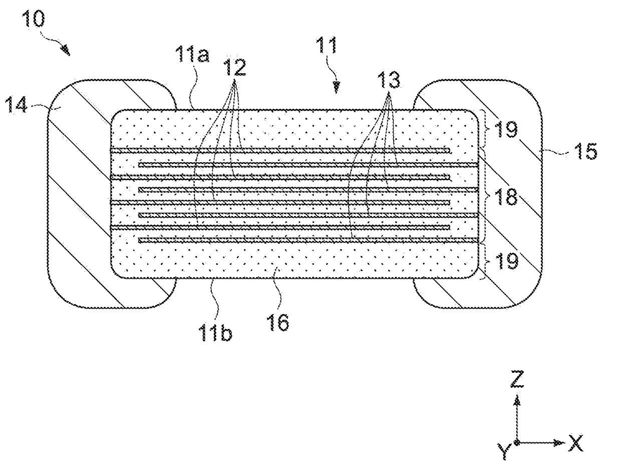
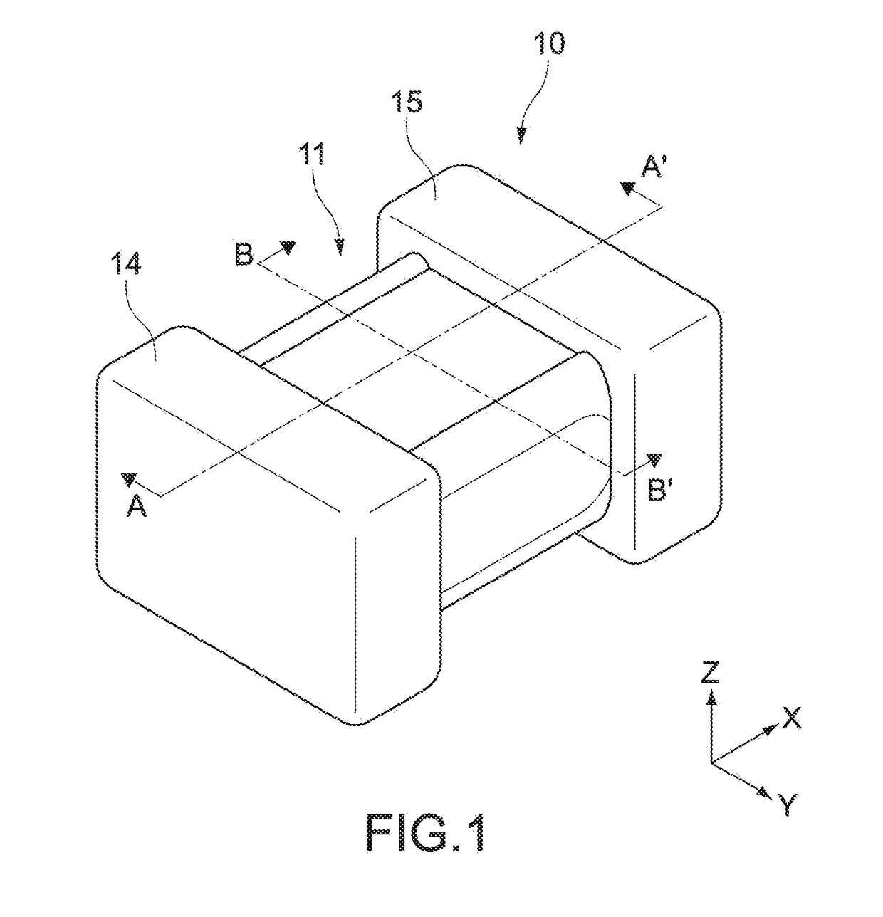
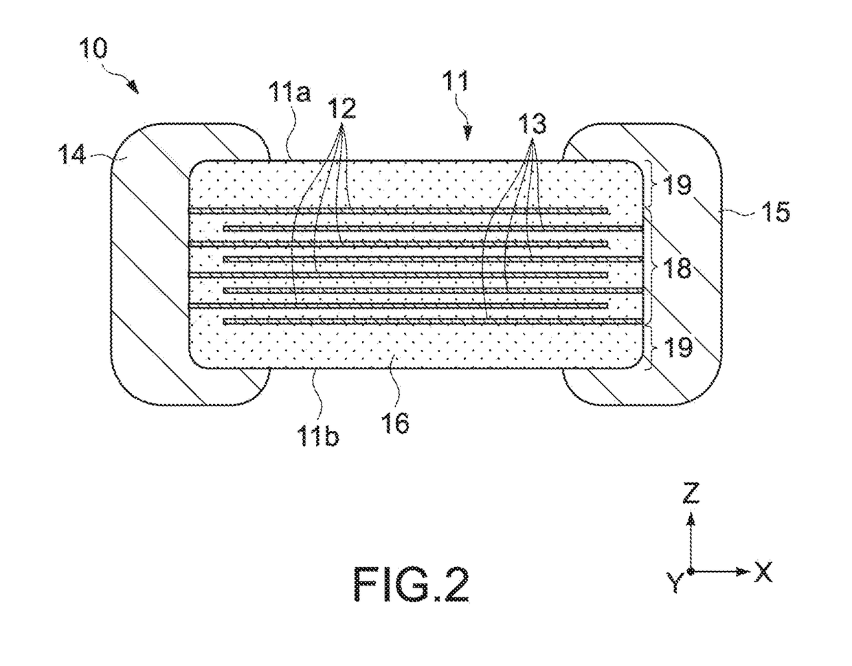
[0050]FIGS. 1 to 3 each show a multi-layer ceramic capacitor 10 according to a first embodiment of the present invention. FIG. 1 is a perspective view of the multi-layer ceramic capacitor 10. FIG. 2 is a cross-sectional view of the multi-layer ceramic capacitor 10 taken along the A-A′ line in FIG. 1. FIG. 3 is a cross-sectional view of the multi-layer ceramic capacitor 10 taken along the B-B′ line in FIG. 1.

[0051]The multi-layer ceramic capacitor 10 includes a body 11, a first external electrode 14, and a second external electrode IS. The first external electrode 14 and the second external electrode 15 are apart from each other and face each other in an X-axis direction while sandwiching the body 11 therebetween.

[0052]The body 11 has two end surfaces (not shown) oriented in the X-axis direction, two side surfaces P and Q oriented in a Y-axis direction, and two main surfaces 11a and 11b oriented in a Z-axis...


PUM

PropertyMeasurementUnit
dielectric constantaaaaaaaaaa
sizeaaaaaaaaaa

Abstract

A method of producing a multi-layer ceramic electronic component includes: preparing a multi-layer chip including ceramic layers laminated in a first axis direction, internal electrodes disposed between the ceramic layers, and a side surface on which the internal electrodes are exposed; applying a ceramic paste to the side surface; and pressing the applied ceramic paste toward the side surface to planarize the applied ceramic paste.

Description

CROSS REFERENCE TO RELATED APPLICATION[0001]This application claims priority under 35 U.S.C. §119 to Japanese Patent Application No. 2016-067679, filed Mar. 30, 2016, which is herein incorporated by references in its entirety.BACKGROUND[0002]The present invention relates to a method of producing a multi-layer ceramic electronic component including side margins provided in a subsequent step, and to a multi-layer ceramic electronic component.[0003]Along with miniaturization of electronic devices and achievement of high performance thereof, there have recently been increasingly strong demands for miniaturization and increase in capacity with respect to multi-layer ceramic capacitors used in the electronic devices. In order to meet those demands, it is effective to enlarge internal electrodes of the multi-layer ceramic capacitor. In order to enlarge the internal electrodes, it is necessary to thin side margins for ensuring insulation properties of the periphery of the internal electrode...

Claims


Application Information

Patent Timeline
Patent Type & Authority Applications(United States)
IPC IPC(8): H01G4/30H01G4/12H01G4/248H01G4/012
CPCH01G4/30H01G4/248H01G4/12H01G4/012
Inventor KOBAYASHI, JOJIKOGURE, TOSHIMITSUKATO, YASUNARIWAKAYANAGI, HIDENORISATO, YOSUKE
Owner TAIYO YUDEN KK
Why Eureka
Try Eureka