This helps you quickly interpret patents by identifying the three key elements:
Problems solved by technology
Method used
Benefits of technology
Benefits of technology
The present patent provides a semiconductor device that can be made smaller while keeping its internal circuit protected from sudden power supply surges. The design method for this semiconductor device is also provided. This invention allows for better protection of the internal circuit while also allowing for smaller components.
Problems solved by technology
For example, there is a strong possibility that an entry of surge from an external connection pad damages elements, such as an input circuit, an output circuit, an input-output circuit, and an internal circuit, and thereby degrades the elements in performance.
In this case, a surge is likely to occur between signals of different power supply domains in the semiconductor device.
When such a surge occurs, an element of a power supply domain where the surge enters may be destroyed.
However, it is difficult for a conventional configuration to protect an internal circuit from the surge occurring between the different power supply domains.
Method used
Image
Click on the blue label to locate the original text in one second.
Reading with bidirectional positioning of images and text.
Examples
embodiment 1
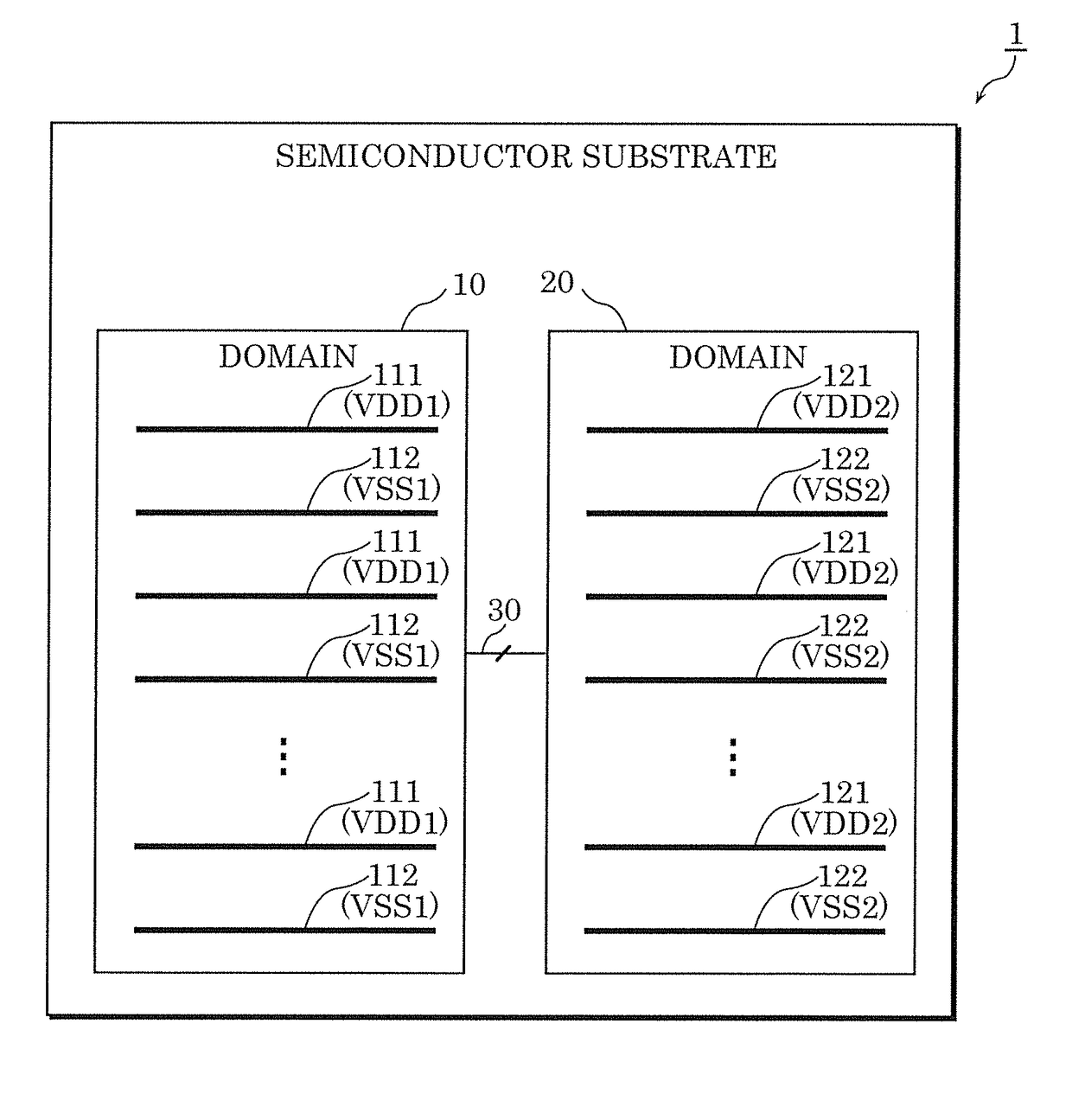
[0037]Firstly, a configuration of semiconductor device 1 according to Embodiment 1 is described in detail. FIG. 1 is a schematiclayout diagram showing an entire configuration of semiconductor device 1, according to Embodiment 1.
[0038]As shown in FIG. 1, semiconductor device 1 includes domain 10 and domain 20 formed on a semiconductor substrate. Semiconductor device 1 includes transistors or other circuit elements (described later) that are formed on a surface of a semiconductor material or an insulating material or formed in the semiconductor material, and thereby has a function of a predetermined electronic circuit. For example, semiconductor device 1 is an LSI (large scale integration), an IC (integrated circuit), a system LSI, a super LSI, or an ultra LSI.
[0039]Domains 10 and 20 are regions to which power supply systems that are mutually different are provided. For example, domain 10 is provided with an analog power supply, and domain 20 is provided with a digital power supply. ...
embodiment 2
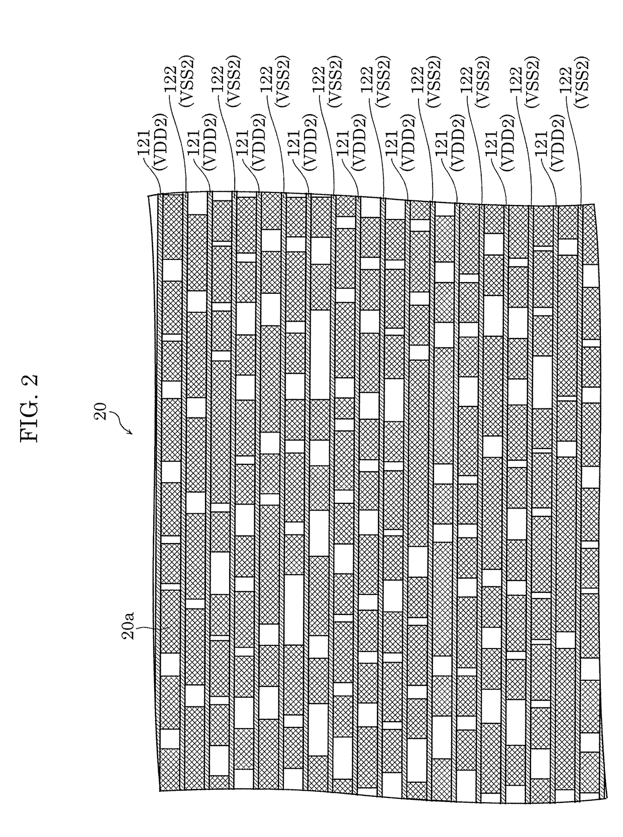
[0093]Next, a configuration of a semiconductor device according to Embodiment 2 is described in detail. FIG. 7 is a layout diagram showing a detailed layout pattern of protection cell 21A and standard cell 24, according to the present embodiment.
[0094]As shown in FIG. 7, the present embodiment is different from Embodiment 1 in that well boundary 40a which is a boundary between N-well 41 and P-well 42 is flexed in protection cell 21A in plan view.
[0095]In the present embodiment, a protection circuit is disposed in a region in which well boundary 40a is flexed. To be more specific, the protection circuit is disposed in one of N-well 41 and P-well 42 that is larger in area in plan view.
[0096]More specifically, in plan view, a part of well boundary 40a in protection cell 21A protrudes toward the power line 121 side more than well boundary 40a located in standard cell 24, as shown in FIG. 7.
[0097]As described above, standard cell 24 usually has, as a most basic circuit configuration, a C...
embodiment 3
[0103]Next, a configuration of a semiconductor device according to Embodiment 3 is described in detail. FIG. 8 is a schematic layout diagram showing an enlarged connection part between domain 10 and domain 20B, according to the present embodiment.
[0104]The present embodiment is different from Embodiment 1 in that a protection circuit includes protection diodes 212B and 222B instead of protection transistors 212 and 222. To be more specific, as shown in FIG. 8, the present embodiment is different from Embodiment 1 in that protection cell 21B includes protection diode 212B instead of protection transistor 212, and that protection cell 22B includes protection diode 222B instead of protection transistor 222.
[0105]Here, a specific configuration of the protection circuit according to the present embodiment is described. It should be noted that the protection circuit formed in protection cell 21B has the same configuration as the protection circuit formed in protection cell 22B. Thus, resi...
PUM
Abstract
A semiconductor device includes a semiconductor substrate having a predetermined region in which a standard cell is disposed, and also includes: a first circuit connected to a first ground power line; a second circuit that is connected to a second ground power line and formed from the standard cells; and a protection circuit interposed and connected between the first circuit and the second circuit. The protection circuit includes: a resistor connected in series between the first circuit and the second circuit; and a protector that is interposed and connected between a node of the resistor on the second circuit side and the second ground power line and clamps a potential difference between the node and the second ground power line to a predetermined voltage or lower. The protection circuit is formed in a protection cell disposed in the predetermined region.
Description
CROSS REFERENCE TO RELATED APPLICATIONS[0001]This application is a U.S. continuation application of PCT International Patent Application Number PCT / JP2015 / 006309 filed on Dec. 18, 2015, claiming the benefit of priority of Japanese Patent Application Number 2015-002650 filed on Jan. 8, 2015, the entire contents of which are hereby incorporated by reference.BACKGROUND1. Technical Field[0002]The present disclosure relates to a semiconductor device which includes a semiconductor substrate having a predetermined region in which a standard cell that is a circuit block defined in size in a predetermined direction is disposed, and to a design method of the semiconductor device.2. Description of the Related Art[0003]With a higher degree of integration achieved by technological development of micromachining and high-density packaging in processing fields in recent years, semiconductor integrated circuit devices (hereinafter, referred to as semiconductor devices) have become more vulnerable to...
Claims
Application Information
Patent Timeline
Application Date:The date an application was filed.
Publication Date:The date a patent or application was officially published.
First Publication Date:The earliest publication date of a patent with the same application number.
Issue Date:Publication date of the patent grant document.
PCT Entry Date:The Entry date of PCT National Phase.
Estimated Expiry Date:The statutory expiry date of a patent right according to the Patent Law, and it is the longest term of protection that the patent right can achieve without the termination of the patent right due to other reasons(Term extension factor has been taken into account ).
Invalid Date:Actual expiry date is based on effective date or publication date of legal transaction data of invalid patent.

