CMOS Compatible Optical Modulators

a technology of optical modulators and compatible optical modules, applied in non-linear optics, instruments, optics, etc., can solve the problems of reducing the drive voltage/energy efficiency, the limit of the optical linewidth of the resonant modulator, and the inability to permit 2-level structures within commercial cmos foundries, etc., to achieve maximum modulation, minimize optical loss, and enhance modulation

Inactive Publication Date: 2017-11-02
UNIV OF COLORADO THE REGENTS OF
View PDF5 Cites 6 Cited by
  • Summary
  • Abstract
  • Description
  • Claims
  • Application Information

AI Technical Summary

Benefits of technology

[0017]The present invention implements traveling wave modulators such as microring modulators driven with a full or partial standing wave excitation and junction geometries designed to maximize modulation and minimize optical loss. Modulators based on longitudinal (often interdigitated) junctions (where the depletion region is orthogonal to the direction of light propagation) along a resonator, and employing full standing or partial standing wave excitation are described. The same concepts are also applied to lateral and vertical junctions where the depletion region is parallel to the direction of light propagation.
[0018]In one embodiment, this modulation is accomplished by the carrier plasma effect in introduced localized doped semiconductor regions and via the electrical control of carrier density in those regions.
[0019]In standing wave operation the optical field presents ma

Problems solved by technology

However, such a structure requires a partial etch step to be carried out in processing the silicon device layer which is not present in native commercial (electronics) CMOS processes.
This aspect does not permit 2-level structures within commercial CMOS foundries as such a step is not present and allowed in the process flow.
This is because partial etch steps must determine the height of the ridge sides

Method used


Image

  • CMOS Compatible Optical Modulators
  • CMOS Compatible Optical Modulators
  • CMOS Compatible Optical Modulators

Examples


Embodiment Construction

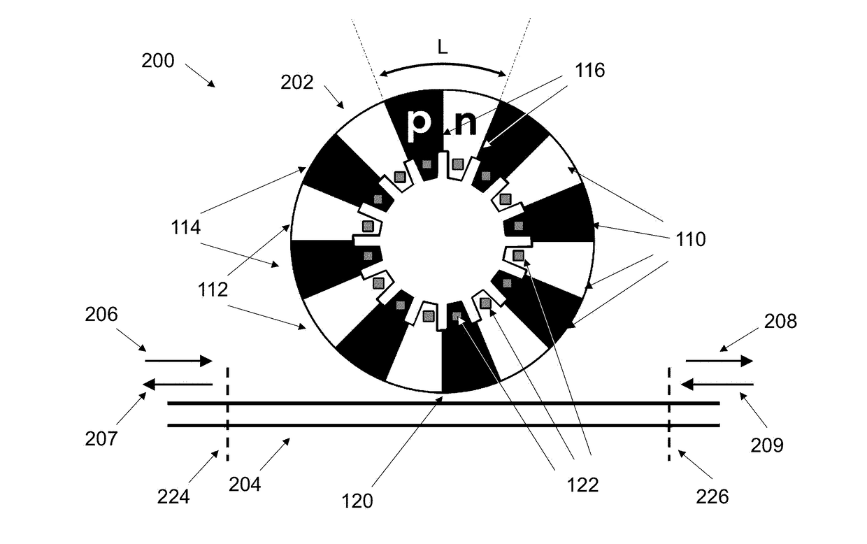
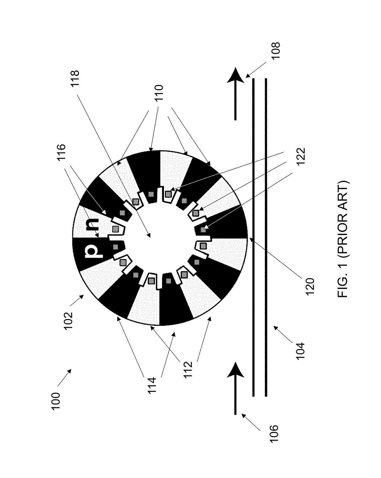
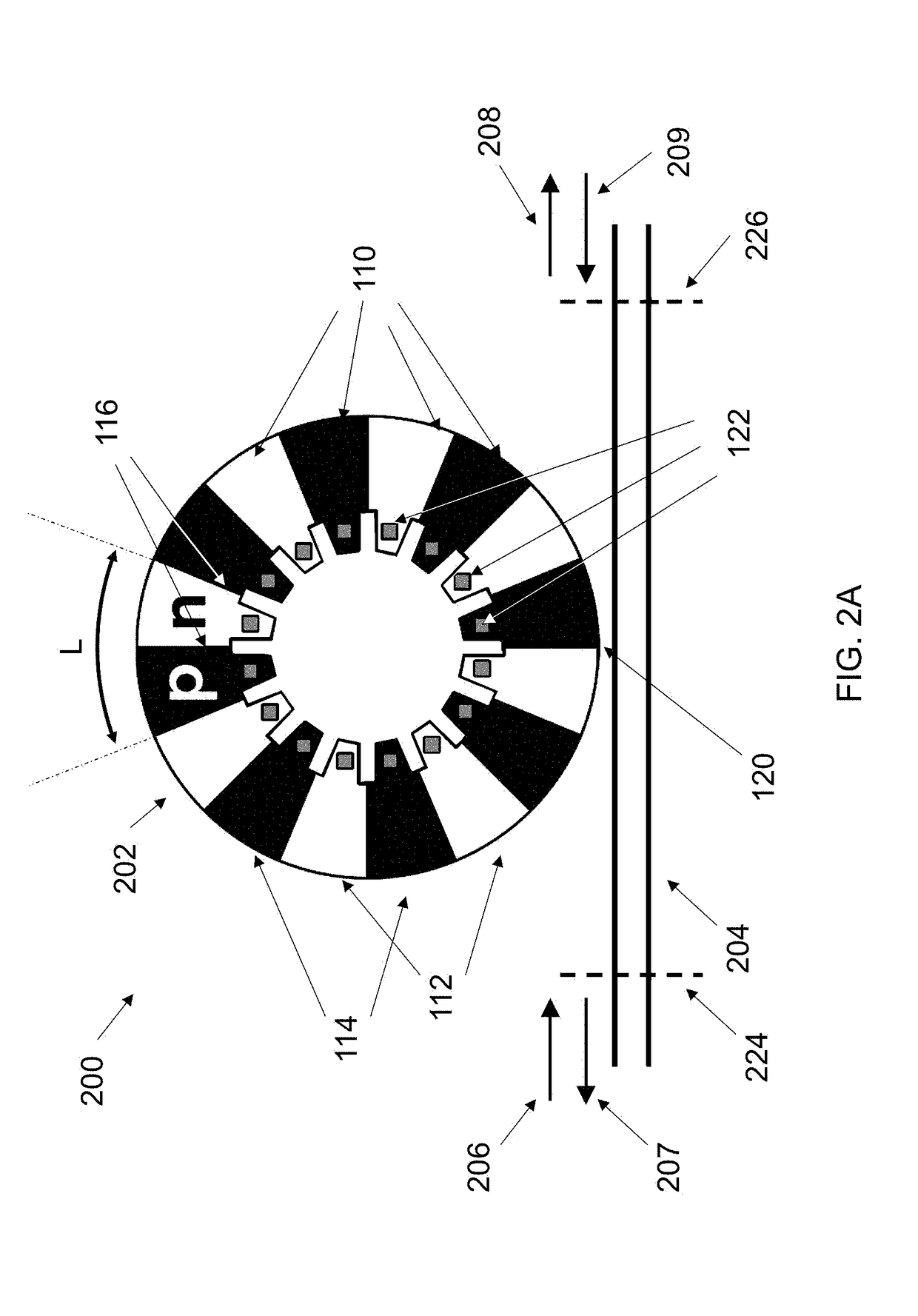
[0033]Various embodiments of the present invention provide different photonic design implementations of a traveling wave resonant cavity and modifications thereof which exploit full or partial standing wave modes. The cavity might have a larger refractive index for the core than the surrounding cladding to achieve strong confinement. The resonant cavity can be made of any semiconductor material which provides the possibility of changing locally its complex (real and imaginary) refractive index, e.g. by modifying the carriers concentration (free carriers plasma effect) or by applying an electric field (Franz-Keldysh effect). While the presented designs are particularly advantageous for lossy phase modulation mechanisms, such as carrier plasma effect, by allowing both enhancement of phase modulation and minimization of loss, it is also of use for loss-only or phase only modulation mechanisms. For the latter, placing the phase mechanism (e.g. electro-optic polymer modulation) into fiel...


PUM


Abstract

Ring modulators based on interdigitated junctions may be driven in full or partial standing wave mode and, active regions (providing the modulation) and light-absorptive regions (e.g. providing electrical conduction) are placed in a pattern inside a resonant cavity in order to match the maxima and minima of the optical field, respectively. The pattern may be periodic to match the periodicity of a typical electromagnetic field which is periodic with the wavelength. It may also be aperiodic in the case that the cross-section or materials are engineered along the direction of propagation such that the propagation constant (and thus wavelength, i.e. optical wave “local periodicity”) change along the propagation direction.

Description

[0001]Provisional application for patent No. 62 / 192,003, filed 13 Jul. 2015 is incorporated herein by reference.[0002]This invention was made with government support under Grant No. HR0011-11-C-0100 awarded by the DARPA program on Photonically Optimized Embedded Microprocessors (POEM). The government has certain rights in this invention.BACKGROUND OF THE INVENTIONField of the Invention[0003]The present invention relates to CMOS compatible optical modulators, and in particular electro-optic modulator or detector devices exploiting field maxima and nulls along the propagation direction of an optical field to opportunely place active regions which may introduce modulation of the local refractive index or absorption properties.Discussion of Related Art[0004]Optical interconnects offer several advantages compared to electrical interconnects in terms of bandwidth, required energy per bit, routing and latency. In order to be a valuable approach commercially, optical interconnects should pr...

Claims


Application Information

Patent Timeline
IPC IPC(8): G02F1/29
CPCG02F1/29G02F2201/06G02F2202/10G02F1/0118G02F1/015G02F1/01708G02F1/2257G02F2203/15G02F1/025G02F1/0156G02F1/0152G02F1/0151G02F1/0155
Inventor POPOVIC, MILOSPAVANELLO, FABIO
Owner UNIV OF COLORADO THE REGENTS OF
Why Eureka
Try Eureka