Sensor including core-shell nanostructure, and method for producing same
a sensor and nanostructure technology, applied in the field of sensors, can solve the problems of insufficiently sensitive nano chemical sensors, unstudied or reported, etc., and achieve the effects of improving the sensitivity of the sensor, reducing the cost and time of producing the sensor, and excellent sensitivity
- Summary
- Abstract
- Description
- Claims
- Application Information
AI Technical Summary
Benefits of technology
Problems solved by technology
Method used
Image
Examples
example 1
Preparing 1 of a Gas Sensor
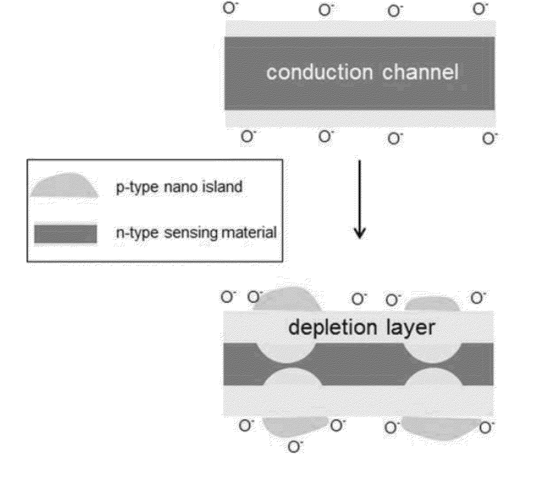
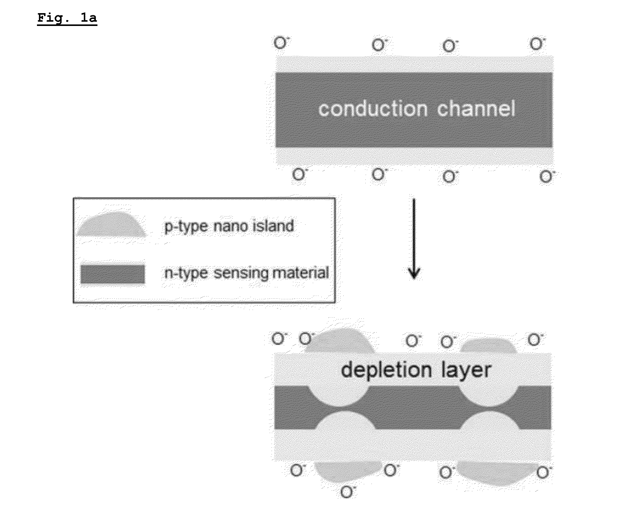
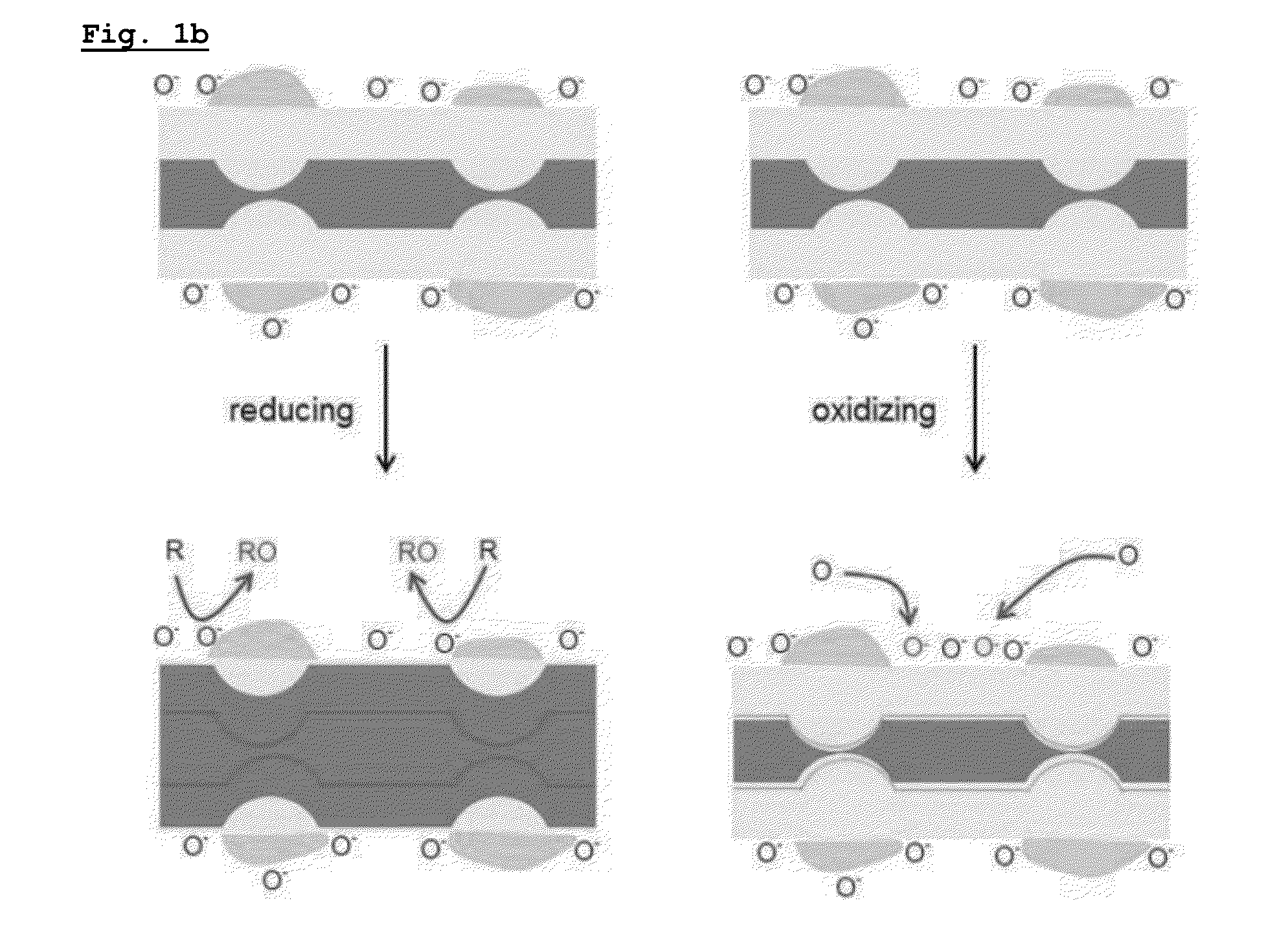
[0203]Cr2O3 nano islands were discretely formed on a surface of a SnO2 nanowire.
[0204]At this time, the forming of the nano islands was performed through processes described below.
[0205]A SnO2 nanowire was selectively grown on a PIEs substrate for 5 minutes by applying a vapor-liquid-solid method (VLS) on a SiO2 (300 nm) / Si substrate on which PIEs (Au 3 nm / Pt 200 nm / Ti 50 nm) were formed. At this time, the Au layer, which is disposed on a top of the PIEs substrate, was used as a catalyst for growing the nanowire, and the Pt layer was used as an electrode. Also, the Ti layer was used for improving a bonding between the substrate and the electrode layer.
[0206]Further, chromium was deposited on the substrate on which the SnO2 nanowire was grown, for 30 seconds by using a DC sputter equipped with a chromium (Cr) target, and the chromium-deposited substrate was heat-treated for 2 hours under an oxygen atmosphere having a temperature of 700° C., and finally, the...
example 2
Preparing 2 of a Gas Sensor
[0207]Except that the sputtering was performed by equipping a titanium (Ti) target instead of the chromium (Cr) target of Example 1, Example 2 was performed in the same manner as Example 1, to prepare a gas sensor in which a SnO2 nanowire was provided on a substrate and TiO2 nano islands were discretely formed on a surface of the SnO2 nanowire.
example 3
Preparing 3 of a Gas Sensor
[0208]Except that the sputtering was performed by equipping a tungsten (Ti) target instead of the chromium (Cr) target of Example 1, Example 2 was performed in the same manner as Example 1 to prepare a gas sensor in which a SnO2 nanowire was provided on a substrate and WiO3 nano islands were discretely formed on a surface of the SnO2 nanowire.
PUM
| Property | Measurement | Unit |
|---|---|---|
| diameter | aaaaa | aaaaa |
| diameter | aaaaa | aaaaa |
| thickness | aaaaa | aaaaa |
Abstract
Description
Claims
Application Information


