Eureka AIR delivers breakthrough ideas for toughest innovation challenges, trusted by R&D personnel around the world.

Semiconductor package

a semiconductor and package technology, applied in the field of semiconductor packages, can solve the problems of inferior heat radiation property, large size of semiconductor packages, and high cost of ceramic caps, and achieve the effects of improving heat radiation property and shielding properties, and reducing the cost of semiconductor packages

Active Publication Date: 2017-11-16
MITSUBISHI ELECTRIC CORP
View PDF4 Cites 8 Cited by
  • Summary
  • Abstract
  • Description
  • Claims
  • Application Information

AI Technical Summary

Benefits of technology

The present invention provides a semiconductor package that is smaller, cheaper, and has better heat radiation and electromagnetic wave shielding properties than conventional configurations. This is achieved by a specific configuration described in the patent text.

Problems solved by technology

However, in the configuration disclosed in Patent Literature 1, the ceramic cap may be expensive.
This fact may bring about a problem that the semiconductor package becomes larger in size.
This structure may bring about a problem that heat radiation property is inferior to that in a case where the IC chip is mounted on a lead frame.

Method used


Image

  • Semiconductor package
  • Semiconductor package
  • Semiconductor package

Examples


embodiment 1

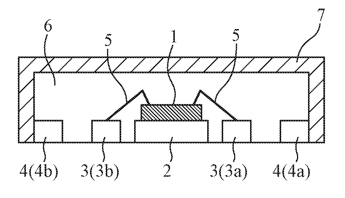
[0021]FIG. 1 is a cross-sectional diagram illustrating a configuration of a semiconductor package according to Embodiment 1 of the present invention.

[0022]The semiconductor package uses a lead frame being thin plate metal, and has a built-in IC chip (electronic component) 1. As illustrated in FIG. 1, the lead frame has a die pad 2, on which the IC chip 1 is fixed, and terminals 3 being internal wires of the semiconductor package. The IC chip 1 is disposed on the top surface of the die pad 2. The die pad 2 is utilized for heat radiation as well as fixing of the IC chip 1.

[0023]The terminals 3 are disposed to surround the die pad 2 on a package plane. The terminals 3 are used for inputting and outputting signals or power. In FIG. 1, two terminals 3a and 3b are depicted. The bottom surfaces of the terminals 3 are exposed to the outside. The terminals 3 are formed to be connectable to a signal terminal or a power supply terminal on a printed circuit board (not illustrated) on which the ...

embodiment 2

[0041]FIG. 4 is a cross-sectional diagram illustrating a configuration of a semiconductor package according to Embodiment 2 of the present invention. The semiconductor package according to the Embodiment 2 illustrated in FIG. 4 is intended to replace, with a terminal (second terminal) 8, the terminal 4 of the semiconductor package according to the Embodiment 1 illustrated in FIG. 1. Since the other configurations are similar to those in the Embodiment 1, the same signs are assigned, and the description thereof will be omitted.

[0042]The terminal 8 is a terminal disposed to surround the terminals 3. The terminals 8 may be discretely disposed in an island-shaped manner, or may be connected to be a series. In the example illustrated in FIG. 4, two terminals 8a and 8b are depicted, each of which is the terminal 8. The bottom surface of the terminal 8 is exposed to the outside. The terminal 8 is formed to be connectable to a ground terminal on the above-described printed circuit board (or...

embodiment 3

[0049]FIG. 5 is a cross-sectional diagram illustrating a configuration of a semiconductor package according to Embodiment 3 of the present invention. The semiconductor package according to the Embodiment 3 illustrated in FIG. 5 is intended to replace, with a terminal (second terminal) 9, the terminal 4 of the semiconductor package according to the Embodiment 1 illustrated in FIG. 1, and also intended to add a connection member 10. Since the other configurations are similar to the Embodiment 1, the same signs are assigned, and the description thereof will be omitted.

[0050]The terminal 9 is a terminal disposed to surround the terminals 3. The terminals 9 may be discretely disposed in an island-shaped manner, or may be connected to be a series. In the example illustrated in FIG. 5, two terminals 9a and 9b are depicted, each of which is the terminal 9. The bottom surface of the terminal 9 is exposed to the outside. The terminal 9 is formed to be connectable to a ground terminal on the a...


PUM


Abstract

A lead frame includes: a second terminal that is disposed to surround terminals on a package plane and can be grounded; and a conductive member that covers molded resin and is electrically connected to the second terminal.

Description

TECHNICAL FIELD[0001]The present invention relates to a semiconductor package that has a function of shielding electromagnetic waves.BACKGROUND ART[0002]Semiconductor packages having various structures are used, each of which contains an electronic component such as an integrated circuit (IC) chip. Among these semiconductor packages, the one having a lead frame is widely used (e.g., a Quad Flat No Lead (QFN) package). The lead frame is made of thin plate metal which is used for fixing the IC chip and also used as an internal wire of the semiconductor package.[0003]In the semiconductor package, such as the QFN package, the IC chip is bonded to a die pad of the lead frame with silver paste, solder, or the like. A terminal of the lead frame and the IC chip are electrically connected via a gold wire or an aluminum wire. After that, the IC chip and the wire are sealed by epoxy resin or the like in order to protect against humidity, dust, and external stress. The semiconductor package is ...

Claims


Application Information

Patent Timeline
Patent Type & Authority Applications(United States)
IPC IPC(8): H01L23/552H01L23/31H01L23/00H01L23/495
CPCH01L23/552H01L23/49582H01L24/97H01L23/3107H01L24/48H01L24/73H01L2224/32245H01L2224/48247H01L2224/73265H01L2224/97H01L21/561H01L23/293H01L23/4952H01L23/49541H01L23/49551H01L24/32H01L24/45H01L2224/45124H01L2224/45144H01L2924/181H01L2924/1815H01L2924/19107H01L2224/85H01L2224/83H01L2924/00012
Inventor MIZUTANI, HIROYUKIISHIBASHI, HIDENORIYOSHIOKA, HIDEHARUISHIDA, KIYOSHI
Owner MITSUBISHI ELECTRIC CORP
Why Eureka
Eureka Blog
Learn More