Supercharge Your Innovation With Domain-Expert AI Agents!

Power module with low stray inductance

a power module and low stray inductance technology, applied in the direction of semiconductor devices, semiconductor/solid-state device details, electrical apparatus, etc., can solve the problems of increasing the switching loss, reducing the controllability of semiconductor switches, and emi emissions, so as to facilitate the provision of contact areas and improve electrical balancing

Active Publication Date: 2017-11-23
AUDI AG +1
View PDF0 Cites 8 Cited by
  • Summary
  • Abstract
  • Description
  • Claims
  • Application Information

AI Technical Summary

Benefits of technology

The invention aims to provide a power module with low stray inductance. This is achieved by designing two nearly mirror symmetric semiconductor switch / metallization area arrangements that share the inner metallization area. This design reduces the number of electrical interconnections and improves current balancing, resulting in a lower internal stray inductance of the power module compared to other arrangements. Additionally, the arrangement of the outer metallization areas, semiconductor switches, and metallization areas is mirror symmetric to the inner metallization area, which causes a highly balanced current and low stray inductance. The DC side of the substrate and power module also provides an outer DC contact area in the L-shaped form, which further helps in providing a contact area for the DC terminal. Connecting the two outer metallization areas electrically inside the power module improves the electrical balancing and reduces unwanted oscillations during switching events. This arrangement also offers a significantly lower terminal stray inductance compared to existing terminal designs without coaxial arrangement.

Problems solved by technology

In an electrical converter, the commutation loop stray inductance causes voltage overshoots during switching, produces EMI emissions by ringing, and increases the switching losses.
Furthermore, experience with wide bandgap semiconductor power modules shows that the ringing in the power circuit may also produce high frequency noise in the gate circuit, thereby decreasing the controllability of the semiconductor switches and requiring a more sophisticated gate driver.
Paralleling of semiconductor chips, however, requires more space for chip placement and signal routing and may therefore result in a higher stray inductance.
The stray inductance of a power module may be to a large part caused by the design of its power terminals.

Method used


Image

  • Power module with low stray inductance
  • Power module with low stray inductance
  • Power module with low stray inductance

Examples


Embodiment Construction

[0008]It is an objective of the invention to provide a power module with low stray inductance.

[0009]This objective is achieved by the subject-matter of the independent claims. Further exemplary embodiments are evident from the dependent claims and the following description.

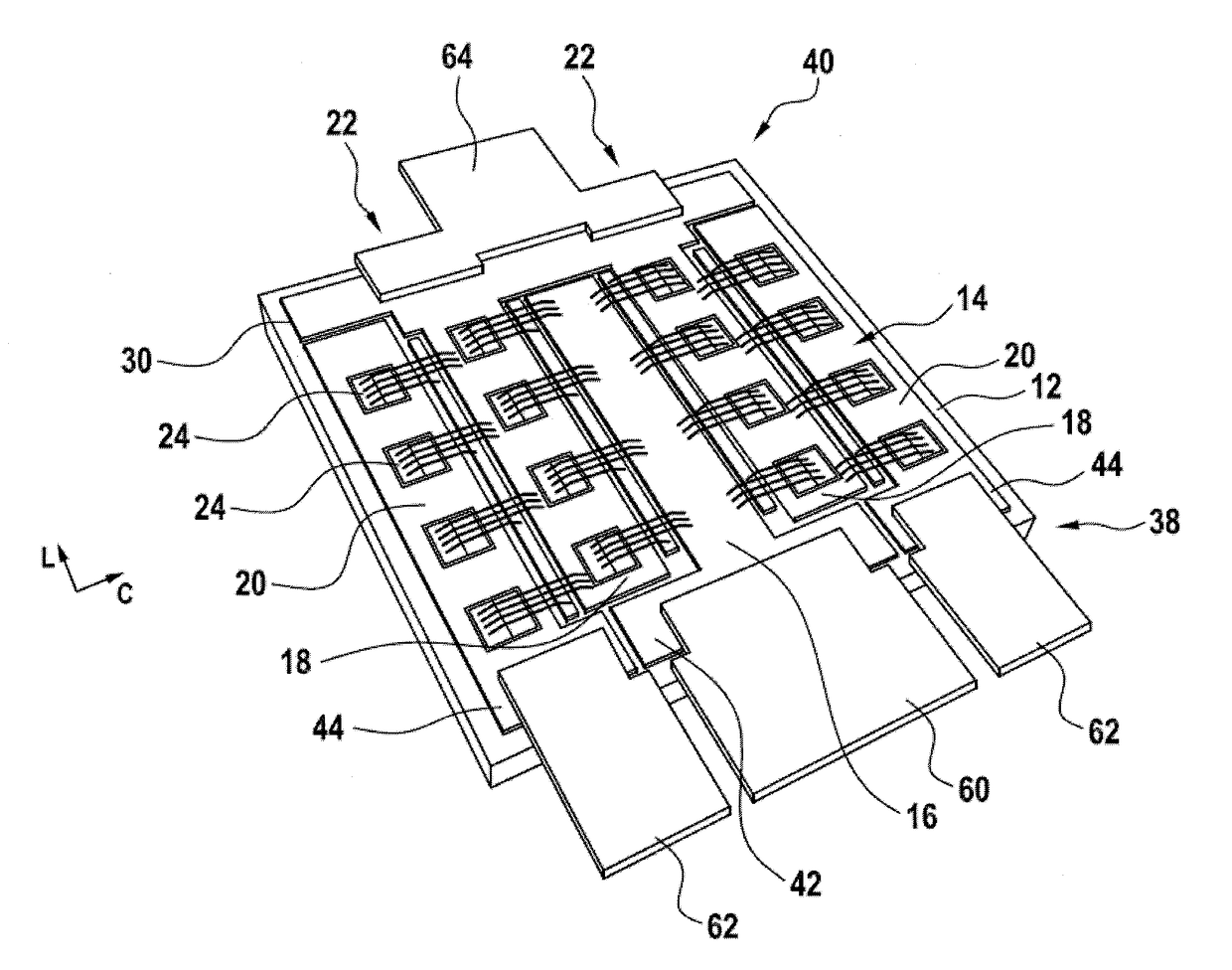
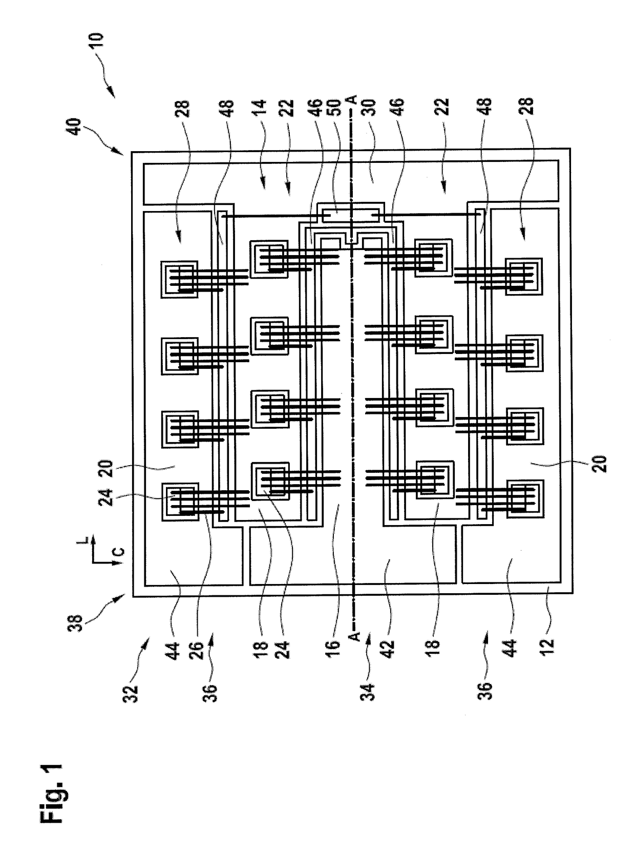
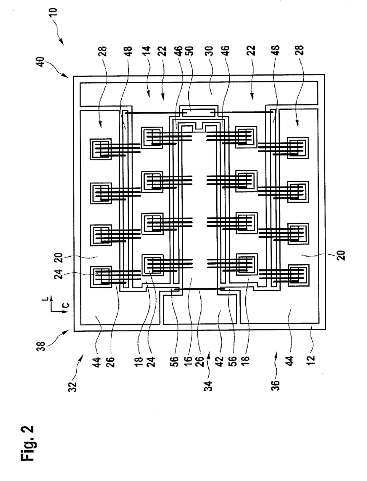
[0010]An aspect of the invention relates to a power module providing a half bridge. A power module may be a device electrically and mechanically interconnecting a plurality of semiconductor switches. Usually, a power module comprises a substrate, which may have metallization layers on one or both sides to which the semiconductor switches are bonded. The substrate and the one or more metallization layers may be a DBC (direct bonded copper) substrate. Furthermore, the power module may comprise terminals, which also may be bonded to the metallization layers. The substrate, semiconductor switches and terminals may be cast into an encasing.

[0011]A half bridge may be an electrical circuit, comprising two switch elements...


PUM


Abstract

A power module providing a half bridge comprises at least one substrate and an inner metallization area, two intermediate metallization areas and two outer metallization areas, each of which extends in a longitudinal direction of the at least one substrate; wherein the two intermediate metallization areas are arranged besides the inner metallization area with respect to a cross direction of the at least one substrate and each outer metallization area is arranged beside one of the two intermediate metallization areas with respect to the cross direction; wherein the power module comprises two inner sets of semiconductor switches, each inner set of semiconductor switches bonded to an intermediate metallization area and electrically connected to the inner metallization area, such that the inner sets of semiconductor switches form a first arm of the half bridge; wherein the power module comprises two outer sets of semiconductor switches, each outer set of semiconductor switches bonded to an outer metallization area and electrically connected to an intermediate metallization area, such that the outer sets of semiconductor switches form a second arm of the half bridge.

Description

FIELD OF THE INVENTION[0001]The invention relates to the field of packaging of power semiconductors. In particular, the invention relates to a power module and to a power module and capacitor arrangement.BACKGROUND OF THE INVENTION[0002]In an electrical converter, the commutation loop stray inductance causes voltage overshoots during switching, produces EMI emissions by ringing, and increases the switching losses. Furthermore, experience with wide bandgap semiconductor power modules shows that the ringing in the power circuit may also produce high frequency noise in the gate circuit, thereby decreasing the controllability of the semiconductor switches and requiring a more sophisticated gate driver. The power module may be part of the commutation loop, therefore minimizing its stray inductance may be important.[0003]Furthermore, power modules for fast switching semiconductors, especially for wide bandgap semiconductors, should have a low stray inductance (below 10 nH) to handle short...

Claims


Application Information

Patent Timeline
Patent Type & Authority Applications(United States)
IPC IPC(8): H01L23/14H01L23/24H01L23/00
CPCH01L23/142H01L23/24H01L2924/30107H01L24/06H01L2924/1304H01L24/48H01L23/481H01L25/16H01L23/5386H01L25/072H02M7/003H01L2224/0603H01L24/49H01L25/18H01L2224/49111H01L2224/49113H01L2224/49175H01L2924/19107H01L23/3121H01L2224/48091H01L2924/00014H01L2924/181H01L2924/13091H01L2924/13055H01L2224/45099H01L2924/00012H01L2924/00
Inventor COTTET, DIDIERTRAUB, FELIX
Owner AUDI AG
Features
  • R&D
  • Intellectual Property
  • Life Sciences
  • Materials
  • Tech Scout
  • Unparalleled Data Quality
  • Higher Quality Content
  • 60% Fewer Hallucinations
Learn More