
Power semiconductor module

a technology of semiconductor modules and semiconductor devices, applied in semiconductor devices, semiconductor/solid-state device details, electrical apparatus, etc., can solve the problems of limiting the maximum achievable switching time, stray inductance of standard planar power modules cannot be easily reduced to values below 5-10 nh, and is often not acceptable, so as to reduce stray inductance, reduce stray inductance, and facilitate module design.

Active Publication Date: 2019-05-07
HITACHI ENERGY LTD
View PDF18 Cites 1 Cited by
  • Summary
  • Abstract
  • Description
  • Claims
  • Application Information

AI Technical Summary

Benefits of technology

The present invention aims to provide a power semiconductor module that has low stray inductance and is easy to build using state of the art techniques. The module design may be simplified in a large amount by using an interposer in case the substrates are located far away from each other.

Problems solved by technology

However, electromagnetic parasitics in the power module give rise to severe switching distortions in power modules, thereby limiting the maximum achievable switching times.
In practice, the stray inductance of standard planar power modules can therefore not easily be reduced to values below ˜5-10 nH.
For fast switching semiconductors with rise-times of ˜10 ns, this value is often not acceptable.
During turn-on of the switch, this voltage leads to a slower commutation and higher switching losses.
During turn-off of the switch, the voltage adds to the already applied DC link voltage and induces an overvoltage, thereby exerting stress on the switch and requiring de-rating.
The impact of stray inductance on total switching losses is complex, but as a general rule, lower inductance also reduces switching losses.
The problem will become even worse for devices from wide band gap semiconductor materials (SiC, GaN) with typically higher output capacitance, see J. Biela, M. Schweizer, S. Waffler and J. W. Kolar, “SiC versus Si—Evaluation of Potentials for Performance Improvement of Inverter and DC-DC Converter Systems by SiC Power Semiconductors,” IEEE Transactions on Industrial Electronics, vol.
This effect is most significant for several paralleled switches, when slightly different coupling coefficients can produce a dramatic current imbalance during switching.

Method used


Image

  • Power semiconductor module
  • Power semiconductor module
  • Power semiconductor module

Examples


Embodiment Construction

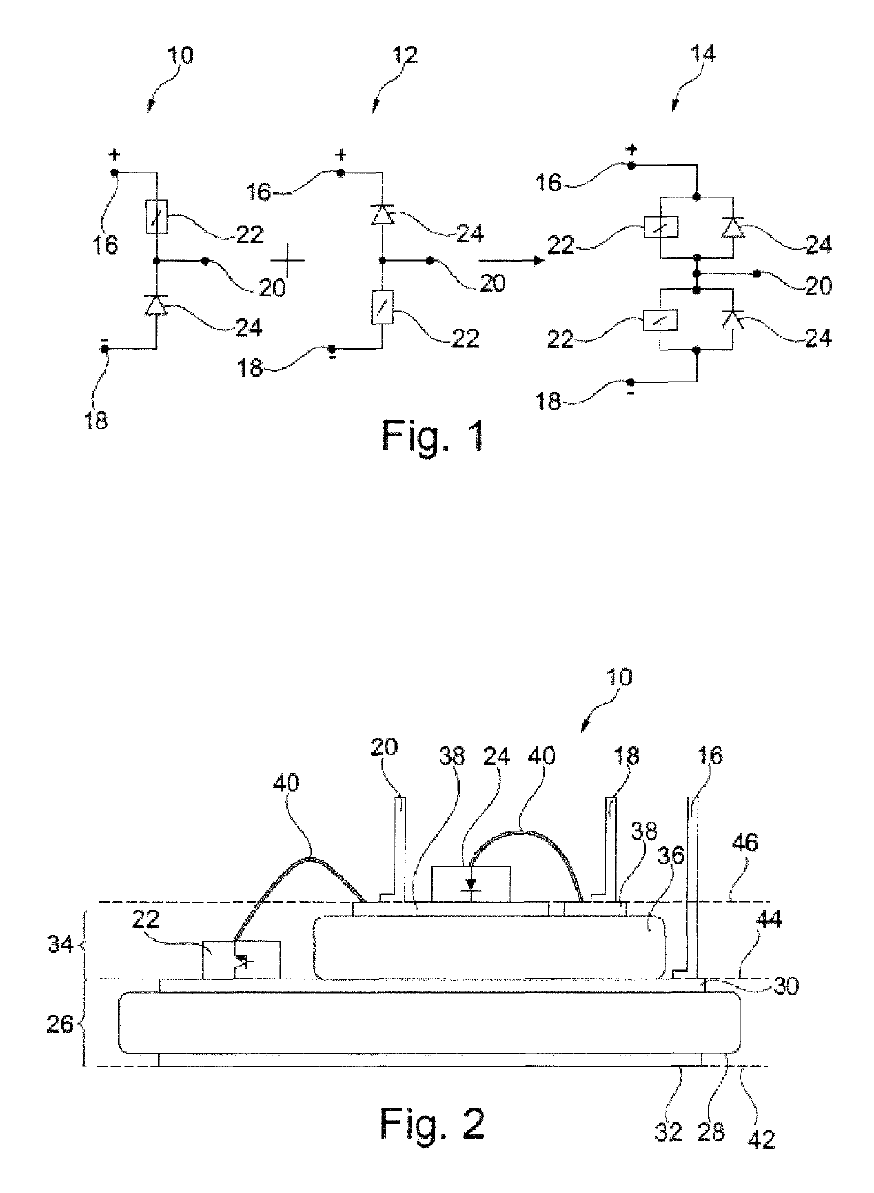
[0084]In FIG. 1, an embodiment of an electronic circuit topology is shown, which may be realized by means of the power semiconductor module according to the invention.

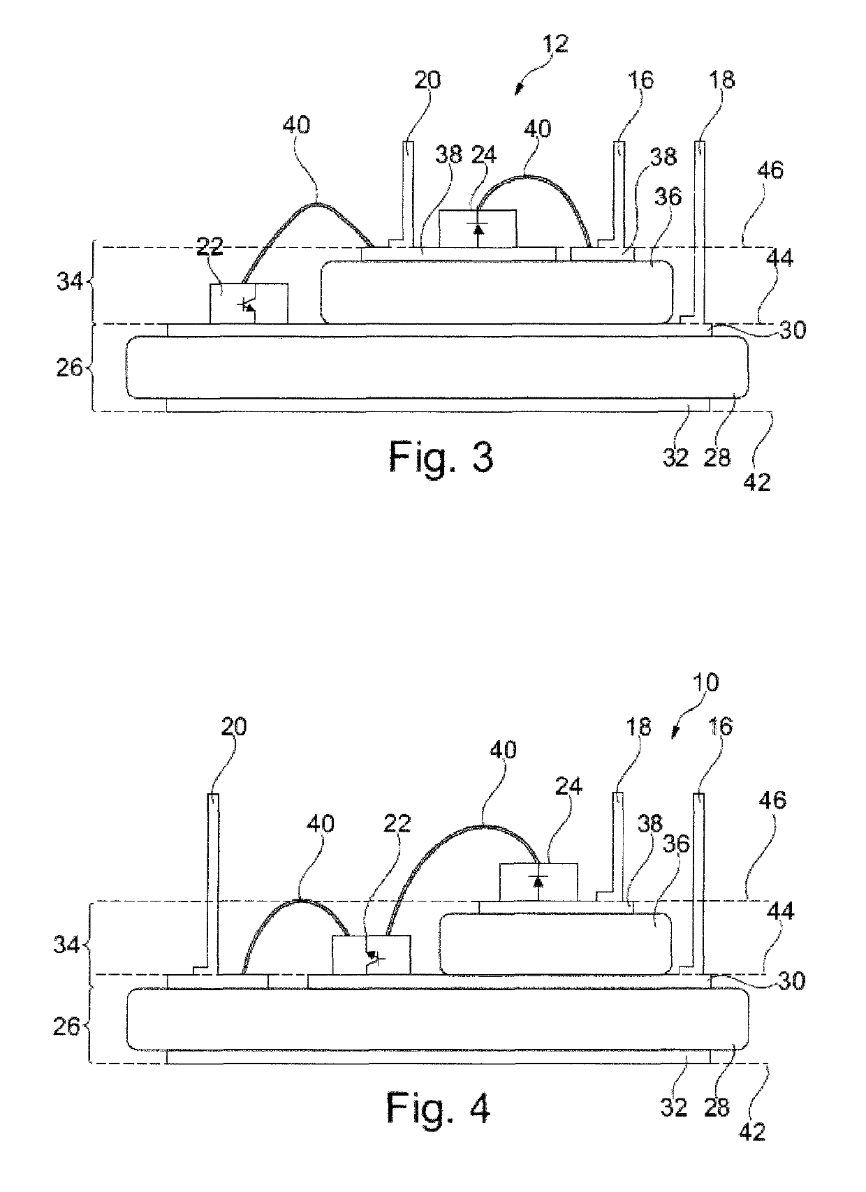
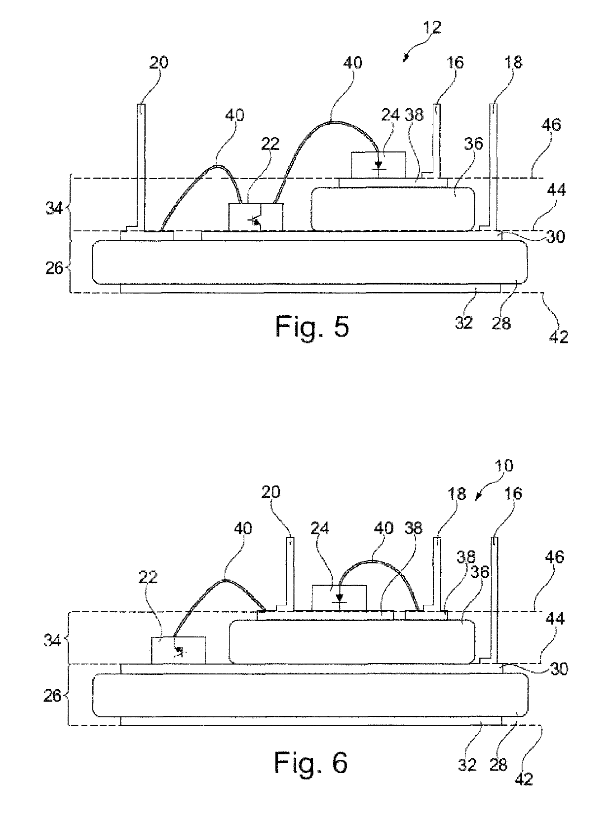
[0085]In detail, a P-cell 10 is shown as well as an N-cell 12, which may form a half-bridge module 14 in a parallel combination, or connection, respectively. Regarding the P-cell 10 and the N-cell 12, these cells comprise a DC+ terminal, or positive DC-connection 16 and a DC− terminal, or negative DC-connection 18, respectively, as well as an AC-connection 20. Further, a transistor 22 working as a switch is provided, which may be formed by a MOSFET, IGBT or the like. Additionally, a diode 24 is provided. Further, the AC-connection 20 is provided which, at the P-cell 10, may connect the circuit to the positive lead of a current-source or inductor and which, at the N-cell, may connect the circuit to the negative lead of a current-source or inductor.

[0086]As stated above, providing low stray inductance in a circuit may be...


PUM


Abstract

The present invention relates to a power semiconductor module, comprising at least two power semiconductor devices, wherein the at least two power semiconductor devices comprise at least one power semiconductor transistor and at least one power semiconductor diode, wherein at least a first substrate is provided for carrying the power semiconductor transistor in a first plane, the first plane lying parallel to the plane of the substrate, wherein the power semiconductor diode is provided in a second plane, wherein the first plane is positioned between the substrate and the second plane in a direction normal to the first plane and wherein the first plane is spaced apart from the second plane in a direction normal to the first plane. The first plane is spaced apart from the second plane in a direction normal to the first plane, whereby the first substrate is based on a direct bonded copper substrate and the first substrate is a direct-bonded copper substrate for carrying the transistor, on which first substrate a layer of a printed circuit board is provided for carrying the diode. Alternatively, the first substrate is a direct-bonded copper substrate for carrying the transistor, on which first substrate a foil is provided for carrying the diode, wherein the foil comprises an electrically insulating main body and an electrically conductive structure provided thereon for carrying the diode. Such a power semiconductor module provides a low stray inductance and / or may be built easily.

Description

TECHNICAL FIELD[0001]The Invention relates to a power semiconductor module. In particular, the invention relates to a power semiconductor module showing a defined arrangement of different power semiconductor devices thereby allowing a significantly decreased stray inductance and thus an improved working behaviour of the power semiconductor module.BACKGROUND ART[0002]Power semiconductor modules are known as such and used in a broad application range. Power semiconductor devices may comprise power semiconductor switches which may switch currents of more than 10 A and / or voltages of more than 500V.[0003]The trend in power semiconductor technology goes into the direction of fast-switching devices. Shorter switching times can be obtained by optimizing silicon (Si) based devices as well as using devices based on wide band gap semiconductor materials, e.g., silicon-carbide (SIC) or gallium-nitrite (GaN). However, electromagnetic parasitics in the power module give rise to severe switching ...

Claims


Application Information

Patent Timeline
Patent Type & Authority Patents(United States)
IPC IPC(8): H01L23/538H01L25/07H01L23/64H01L29/00H01L23/498H01L23/373
CPCH01L23/5385H01L23/645H01L25/072H01L29/00H01L23/3735H01L23/49811H01L2924/19107H01L2224/48091H01L2224/48137H01L2224/49111H01L2924/00014
Inventor TRAUB, FELIXMOHN, FABIANSCHUDERER, JUERGENKEARNEY, DANIELKICIN, SLAVO
Owner HITACHI ENERGY LTD
Learn More