Power electronics module

a technology of power electronics and electronics modules, applied in the direction of electrical apparatus, semiconductor devices, semiconductor/solid-state device details, etc., can solve the problems of complex manufacturing sequence involving a plurality of individual bond layer interfaces and materials, considerable electromagnetic coupling, etc., to reduce the footprint of the power electronics module's semiconductor chips, simplify the bonding of the semiconductor chip stack, and improve manufacturability

Active Publication Date: 2021-03-25
AUDI AG
View PDF0 Cites 1 Cited by
  • Summary
  • Abstract
  • Description
  • Claims
  • Application Information

AI Technical Summary

Benefits of technology

[0032]This may result in a stacked semiconductor chip arrangement reducing the footprint of the semiconductor chips of the power electronics module. Furthermore, the bonding preform may be used as a bond spacer, i.e. may have a height that the first semiconductor chip and the second semiconductor chip are spaced as far apart such than voltage clearing and clearance demands are fulfilled.
[0033]Furt...

Problems solved by technology

Although the footprint of the semiconductor chips may be reduced by die stacking, other on-board components and electrical conductors are still arranged beside the die stack and may result in further considerable footprint an...

Method used


Image

  • Power electronics module
  • Power electronics module
  • Power electronics module

Examples


Embodiment Construction

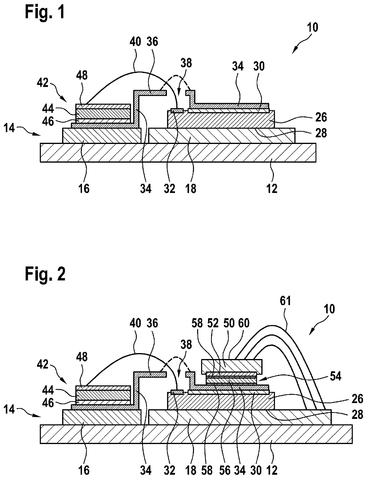
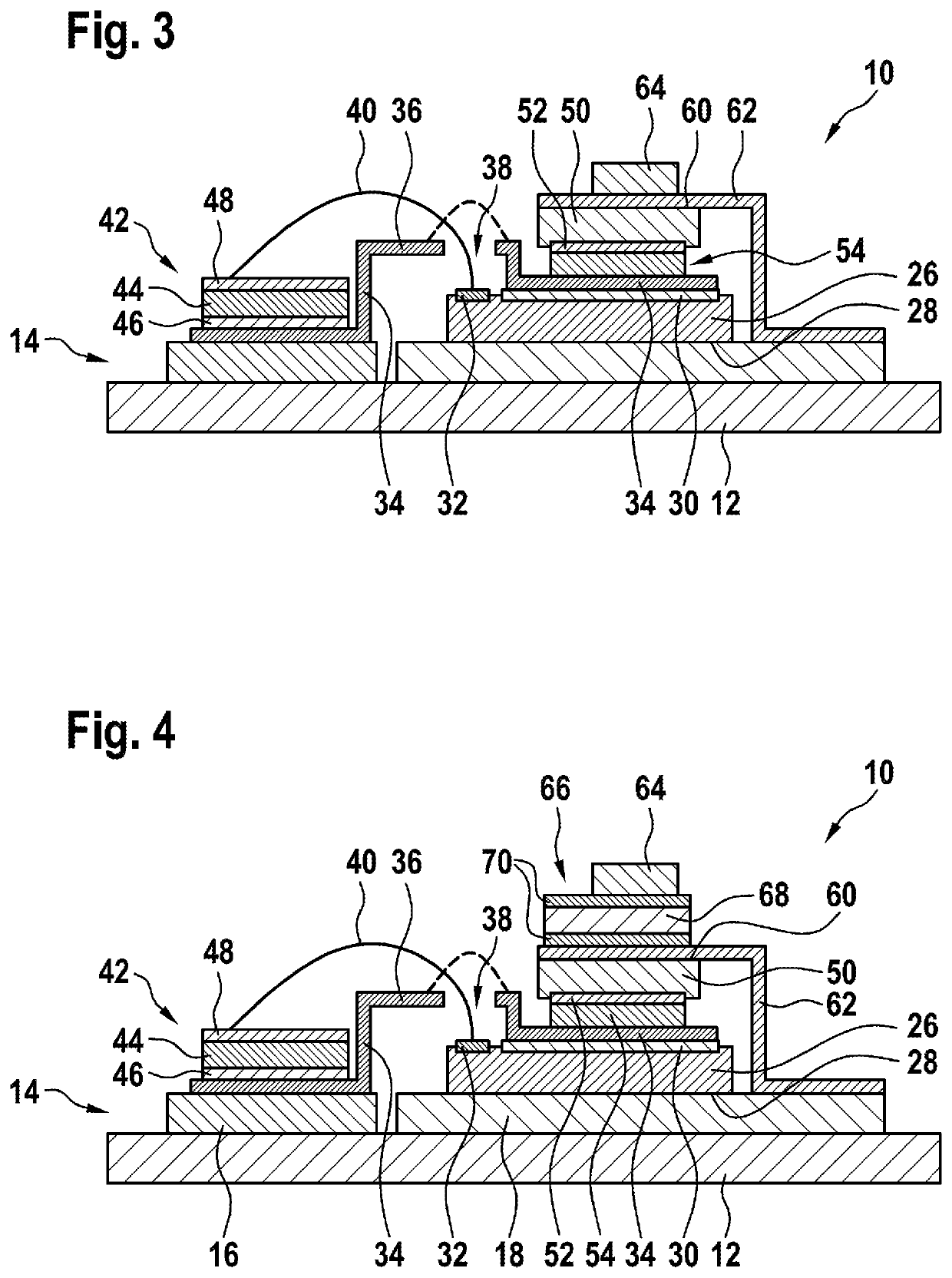
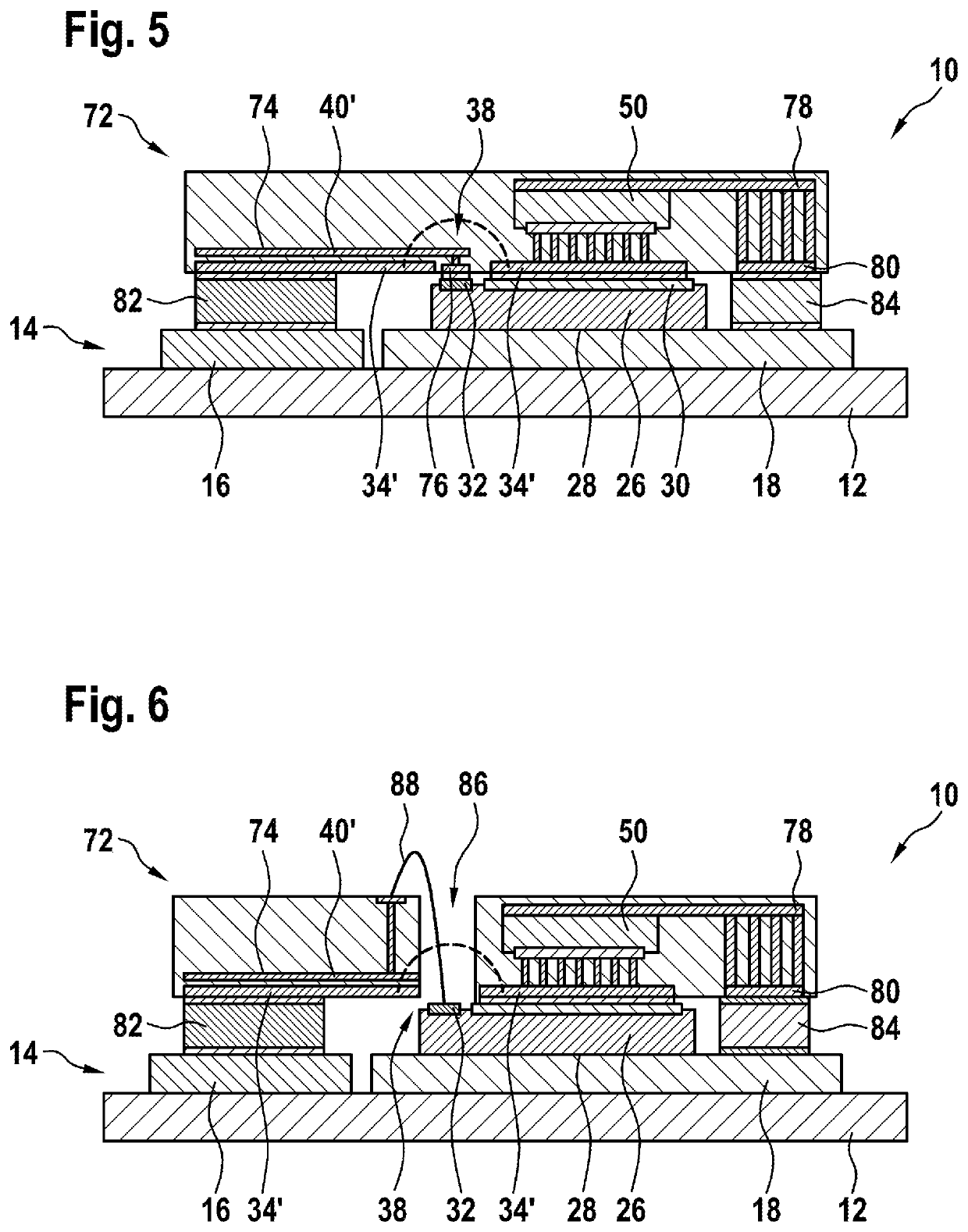
[0007]It is an objective of the invention to provide a power electronics module with enhanced power density having a low stray inductance generated by the electrical interconnections of the semiconductor chips provided by the power electronics module. It is a further objective of the invention to simplify the manufacturing of a power electronics module.

[0008]These objectives are achieved by the subject-matter of the independent claim. Further exemplary embodiments are evident from the dependent claims and the following description.

[0009]The invention relates to a power electronics module. A power electronics module may be any assembly mechanically and electrically supporting one or more semiconductor chips. It has to be noted that the term power may be related to modules and / or semiconductor chips, which are adapted for processing a voltage of more than 100 V and / or than 10 A.

[0010]According to an embodiment of the invention, the power electronics module comprises: a substrate with ...


PUM


Abstract

A power electronics module includes a substrate with a substrate metallization layer, which is separated into conducting areas for providing conducting paths for the power electronics module; a semiconductor switch chip bonded with a first power electrode to a first conducting area of the substrate metallization layer; a conductor plate bonded to a second power electrode of the semiconductor switch chip opposite to the first power electrode.

Description

FIELD OF THE INVENTION[0001]The invention relates to a power electronics module.BACKGROUND OF THE INVENTION[0002]Power electronics modules containing solid-state switching devices, such as IGBTs or Power-MOSFETs, are used in various power electronics applications to switch or rectify electric currents. An important and fast growing application is converter systems for electric or hybrid electric vehicles. A typical six-pack module for such applications may have a voltage rating of up to 1200 V and a current rating of several 100 A. Since the installation space in electric vehicles is usually very limited and geometrically constrained, it is of high advantage if power electronics modules and converters of the electrical drivetrain are as compact as possible to allow for flexible installation.[0003]One approach to increase the power density of a power electronics module is die stacking, i.e., leaving the traditional two-dimensional circuit layout of side-by-side arrangement of semicon...

Claims


Application Information

Patent Timeline
IPC IPC(8): H01L25/11H01L23/498H01L23/492H01L23/00
CPCH01L25/112H01L23/49822H01L23/492H01L2224/29582H01L24/29H01L23/49833H01L2224/48155H01L24/48H01L2224/40095H01L2224/84447H01L2224/8484H01L23/34H01L24/20H01L24/37H01L24/40H01L24/41H01L25/071H01L25/074H01L25/117H01L2223/6627H01L2224/29339H01L2224/32014H01L2224/37147H01L2224/4824H01L2224/4826H01L2224/48491H01L2224/83101H01L2224/83447H01L2224/83801H01L2224/83825H01L2224/8384H01L2924/00014H01L2924/09701H01L2924/10272H01L2924/1203H01L2924/13055H01L2924/13091H01L2924/19104H01L2224/41174H01L2924/1301H01L2924/15787H01L2224/2612H01L2224/73221H01L2224/05599H01L2224/45099H01L2224/45015H01L2924/207
Inventor APELSMEIER, ANDREASASAM, JOHANN
Owner AUDI AG
Why Eureka
Try Eureka