Light-emitting device and method of manufacturing the same

a technology of light-emitting devices and manufacturing methods, which is applied in the direction of semiconductor devices, basic electric elements, electrical apparatus, etc., can solve the problems of deterioration of light-emitting devices, inability to easily dissipate the heat generated in packages, and dissipation of heat generated, so as to improve thermal properties and electrical connection properties.

Active Publication Date: 2017-11-23
SEOUL VIOSYS CO LTD
View PDF2 Cites 4 Cited by
  • Summary
  • Abstract
  • Description
  • Claims
  • Application Information

AI Technical Summary

Benefits of technology

[0022]The present invention has been made in order to solve the above-described problems occurring in the prior art, and it is an object of the present invention to provide a light-emitting device having improved thermal properties and electrical connection properties.

Problems solved by technology

The realization of high output of light-emitting devices requires high power supply and causes problems associated with the dissipation of the heat generated.
Particularly, when the heat generated in a light-emitting device is not smoothly dissipated to the outside, it may result in the deterioration of the light-emitting device.
However, these ceramic materials have a problem in that they do not easily dissipate the heat generated in packages.
In addition, the ceramic materials have a problem in that a separate reflective material needs to be provided below a light-emitting chip so that the light generated in packages is easily emitted to the outside.
However, the use of a polymer material as a molding material makes it difficult to ensure heat dissipation properties, even when a frame made of a metal material is used.
The above-described configuration has a problem in that, because the molded portion 3 forming the sidewall of the light-emitting device cannot easily dissipate the heat generated in the package, the heat transfer properties of the light-emitting device are deteriorated.
Moreover, the decrease in heat transfer to the outside leads to deterioration in the light emitting properties of the light-emitting chip.
In addition, because the molded portion 3 forming the sidewall of the package is made of a black polymer material, it cannot sufficiently reflect the light emitted.
Particularly, when the light-emitting device emits light in the ultraviolet region, the light reflecting properties of the package will be deteriorated due to the frame 1 made of a metal material or the molded portion 3 made of a black polymer material, and the reliability of the light emitting device will be deteriorated due to the low heat transfer properties of the package.
Additionally, if the frame 1 is completely made of a metal such as Al in order to increase the reflectivity, a chip or a submount is mounted on the frame 1 using an Ag paste containing an organic material such as epoxy or silicone, because soldering is impossible as a Sn-based solder is not bonded onto the Al frame.
However, when the chip or the submount is mounted using the Ag paste containing the organic material as described above, the organic material will be influenced by the light (particularly UV light) from the chip for a long period of time, and thus the Ag paste will be delaminated from the frame 1, or the chip or the submount will be delaminated from the Ag paste, resulting in deterioration in the reliability of the device.
However, the conventional ceramic package comprising the glass lens placed directly on the upper end of the cavity is not satisfactory in terms of optical efficiency and light intensity, because light extraction is performed through the lens spaced away from the light-emitting device.
However, the STEM packages are not difficult to produce using automatic systems, and thus cannot be produced in large amounts.

Method used


Image

  • Light-emitting device and method of manufacturing the same
  • Light-emitting device and method of manufacturing the same
  • Light-emitting device and method of manufacturing the same

Examples


embodiments

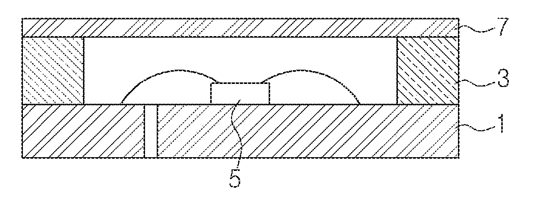
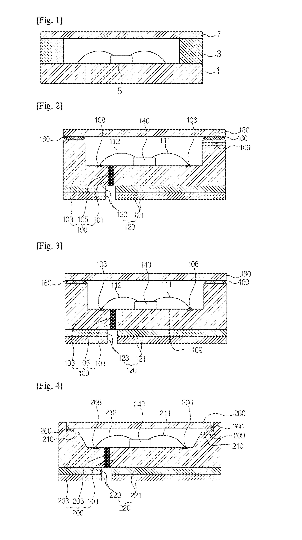
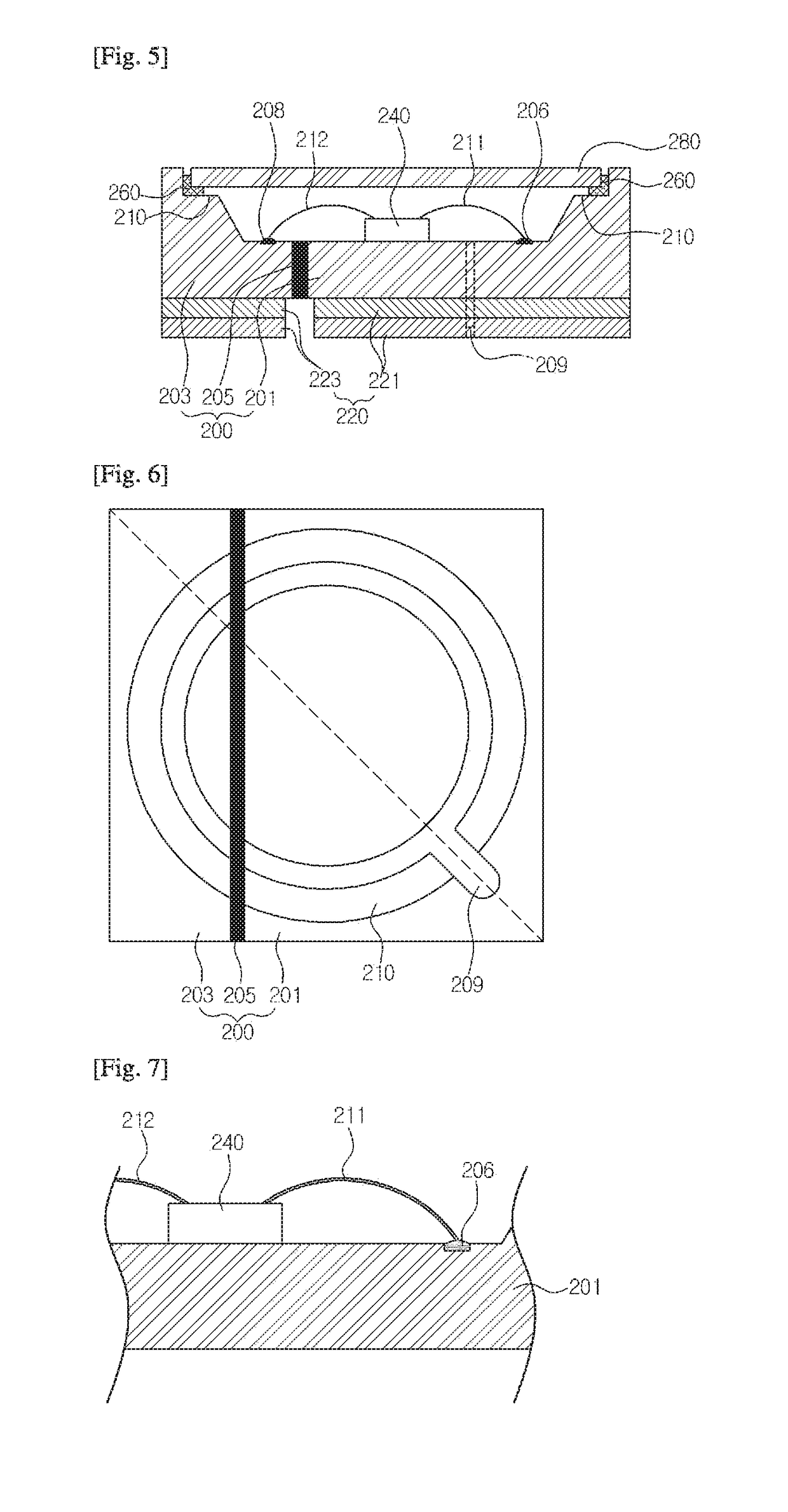
[0168]FIG. 2 is a cross-sectional view showing a light-emitting device according to an embodiment of the present invention.

[0169]Referring to FIG. 2, the light-emitting device according to this embodiment comprises a frame portion 100, an electrode portion 120, a light-emitting portion 140, a buffer portion 160 and a window portion 180.

[0170]The frame portion 100 has a first frame 101, a second frame 103 and an insulating separation layer 105. The frame portion 100 has a depressed central portion. Thus, the internal space defined by the frame 100 includes a light-emitting portion 140, and the light-emitting portion 140 is sealed by the buffer portion 160 and the window portion 180. Thus, the frame portion 100 defines the bottom and sidewall of the light-emitting device.

[0171]The first frame 101 is made of a metal material and preferably has aluminum or an aluminum alloy. The light-emitting portion 140 is provided on the first frame 101. Also, the first frame 101 forms the bottom and...


PUM


Abstract

A light-emitting diode package includes a frame portion with a chip-mounting region defined in an upper portion thereof, and first and second frames spaced apart from each other. A light-emitting diode is mounted on at least a portion of the chip-mounting region with a bonding layer interposed therebetween. The frame portion includes a depressed portion formed on an upper surface thereof, and the depressed portion includes the chip-mounting region defined on a bottom thereof. The depressed portion also includes a step portion disposed at an outer upper end thereof.

Description

CROSS-REFERENCE TO RELATED APPLICATIONS[0001]This application is a continuation of U.S. patent application Ser. No. 14 / 981,301, filed on Dec. 28, 2015, which is a continuation of U.S. patent application Ser. No. 14 / 002,966, filed on Sep. 3, 2013, now issued as U.S. Pat. No. 9,240,524, which is the National Stage entry of International Application No. PCT / KR2013 / 001739, filed on Mar. 5, 2013, and claims priority from and the benefit of Korean Patent Application No. 10-2012-0022476, filed on Mar. 5, 2012, Korean Patent Application No. 10-2012-0024644, filed on Mar. 9, 2012, Korean Patent Application No. 10-2012-0024700, filed on Mar. 9, 2012, and Korean Patent Application No. 10-2013-0002435, filed on Jan. 9, 2013, all of which are hereby incorporated by reference for all purposes as if fully set forth herein.BACKGROUNDField[0002]The present invention relates to a light-emitting device comprising a light-emitting device and a manufacturing method thereof.Discussion[0003]Light-emitting...

Claims


Application Information

Patent Timeline
Patent Type & Authority Applications(United States)
IPC IPC(8): H01L33/48H01L33/58H01L33/62H01L25/075
CPCH01L33/483H01L33/58H01L33/48H01L33/486H01L2224/48091H01L2933/0066H01L2933/0033H01L33/62H01L25/0753H01L2924/00014
Inventor PARK, JUN YONGJUNG, HEE CHEULPARK, IN KYUSUH, DAEWOONG
Owner SEOUL VIOSYS CO LTD
Why Eureka
Try Eureka