Silicon-based optical pulse modulation device and its application

A pulse modulation and device technology, applied in laser parts, lasers, electrical components, etc., can solve the problems of difficult to achieve communication wavelength optical modulation, difficult to achieve passive modulation devices, and low probability of electronic transition, achieve superior performance, and is conducive to Integrated and beneficial to industrialized production

Active Publication Date: 2018-08-24
济南晶众光电科技有限公司
View PDF3 Cites 0 Cited by
  • Summary
  • Abstract
  • Description
  • Claims
  • Application Information

AI Technical Summary

Problems solved by technology

Commonly used semiconductor saturable absorbers mainly include saturable absorber mirror (SESAM) and gallium arsenide (GaAs) devices. In addition to the very complicated manufacturing process, these two devices are also difficult to achieve communication wavelengths of 1.3 μm and 1.5 μm. Light modulation, and it is difficult to form an integrated device compatible with silicon due to different materials
[0003] In order to meet the needs of integration and the modulation of light in the communication band, silicon-based modulation devices are the ideal choice, but silicon single crystal is an indirect bandgap semiconductor material, and its electron transition probability in silicon semiconductors is small, so it is difficult to realize passive modulation devices

Method used


Image

  • Silicon-based optical pulse modulation device and its application
  • Silicon-based optical pulse modulation device and its application
  • Silicon-based optical pulse modulation device and its application

Examples


Embodiment 1

[0037] Embodiment 1, doping 32 Single-doped silicon-based optical pulse modulation device based on S

[0038] A silicon wafer with a thickness of 0.5mm made of single crystal silicon has a size of 6mm×6mm. Doped at room temperature by ion implantation 32 S, 32 The S implant energy is 80keV, and the implant dose is 3×10 15 cm -2 . The ion implantation process is based on the prior art, see "Enhancing the Infrared Photoresponse of Silicon by Controlling the FermiLevel Location within an Impurity Band", Advanced Functional Materials, DOI: 10.1002 / adfm.201303820.

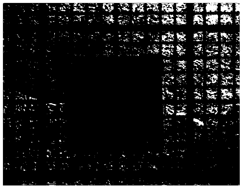
[0039] Pulse modulation devices can be fabricated into rectangular or circular shapes, depending on the needs of the application. Physical photos such as figure 1 As shown, the photo is shown as a rectangle.

Embodiment 2

[0040] Embodiment 2, doping 32 S and 11 Double-doped silicon-based optical pulse modulation device of B

[0041] There are three silicon wafers with a thickness of 0.5mm made of monocrystalline silicon, and the sizes are 4mm×4mm, 7mm×7mm, and 10mm×10mm.

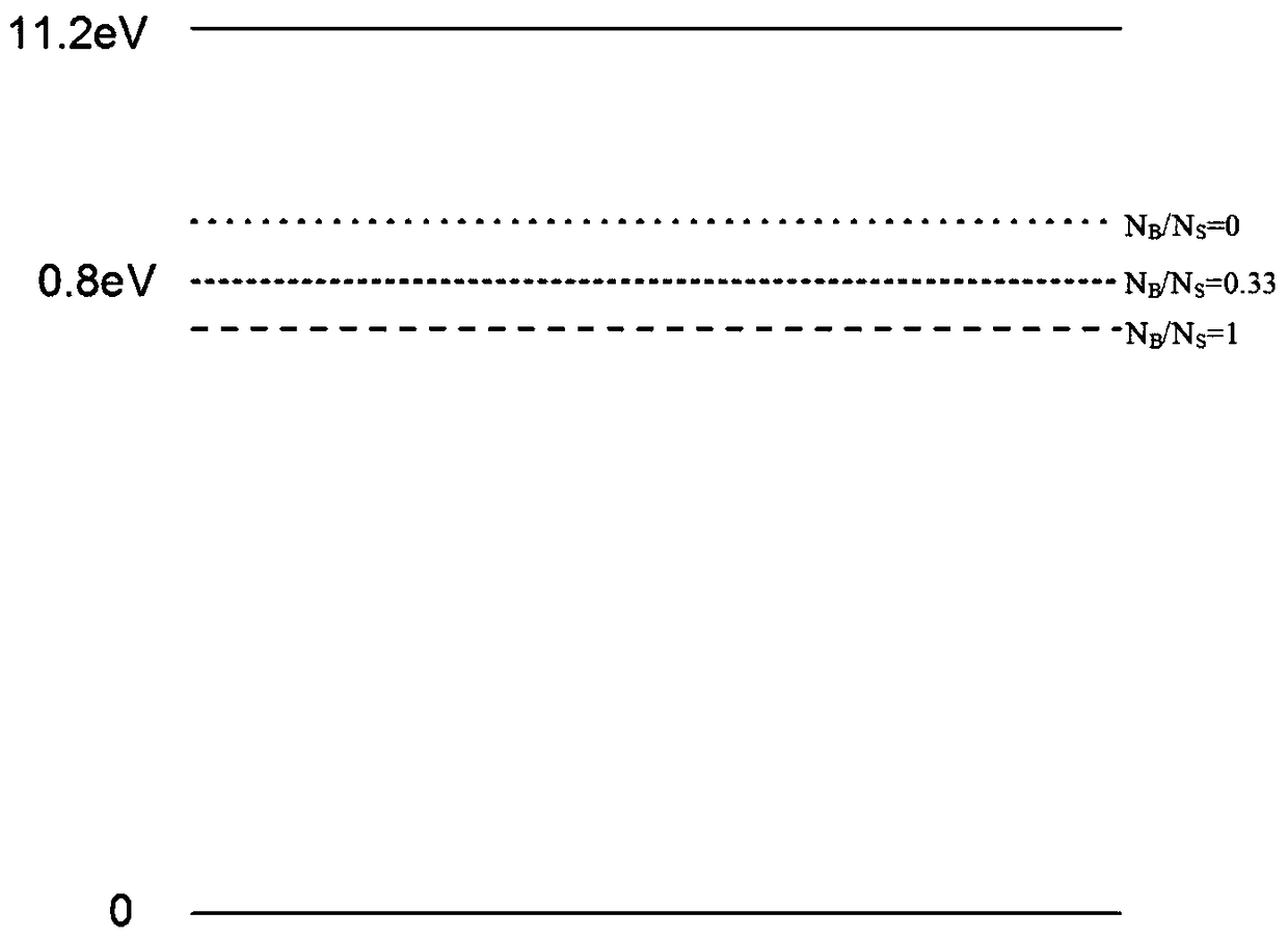
[0042] At room temperature, the above three silicon wafers were doped by ion implantation 32 S and 11 B: Three silicon wafers of different sizes are implanted first 32 S, 32 The S implant energy is 60keV, and the implant dose is 3×10 15 cm -2 ; then, inject 11 B, 11 The injection energy of B is 40keV, 11 B injection doses are 0, 1×10 15 cm -2 and 3×10 15 cm -2 . Pulse modulation devices can be fabricated into rectangular or circular shapes, depending on the needs of the application.

[0043] Made 32 S and 11 The distribution of the Fermi level of B double-doped silicon wafer is as follows figure 2 shown. Among them, 0.8eV corresponds to a laser wavelength of 1550nm.

Embodiment 3

[0044] Embodiment 3, doping 32 Single-doped silicon-based optical pulse modulation device based on S

[0045] As described in Embodiment 1, the difference is that the silicon wafer made of single crystal silicon has a thickness of 1 mm and a size of 8 mm×8 mm. 32 The S implant energy is 100keV, and the implant dose is 5×10 15 cm -2 .


PUM


Abstract

The invention relates to a silicon-based optical pulse modulator device and application. The silicon-based optical pulse modulator is characterized in that monocrystalline silicone is processed into a silicon wafer, 32S or 32S and 11B together are injected into the silicon wafer by an ion injection method, the silicon wafer is subjected to twin polishing, and a high-penetration medium film of 1.3-1.6 micrometers is plated or not on the surface of the silicon wafer. The silicon-based optical pulse modulator device is used for a laser, pump light passes a laser gain medium and then passes a silicon-based optical pulse component, and a front endoscope in front of the laser gain medium and a rear endoscope behind the silicon-based optical pulse component constitute a resonance cavity. The silicon-based optical pulse modulator device is used for adjusting loss of laser of 1.3-1.6 micrometers. The silicon-based optical pulse modulator device is simple to manufacture and low in cost, miniaturization of products and industrialized production are facilitated.

Description

technical field [0001] The invention relates to a silicon-based optical pulse modulation device and its application, belonging to the technical field of laser devices. Background technique [0002] Silicon single crystal is the foundation and core of the optoelectronic industry. Computers, detectors, semiconductors and other fields are designed based on silicon single crystal electrical devices. Especially in the computer field, in order to further increase the computing speed, silicon-based optoelectronics has become a new discipline, including silicon light-emitting devices, silicon active modulation devices, etc. Passive modulation devices have the advantages of small size, simple structure, and easy integration, and are the first choice for pulsed optical devices. Passive modulation mainly uses the nonlinear saturable absorption effect of semiconductor materials, that is, when strong light is irradiated, the electrons in the valence band will all jump to the conduction ...

Claims


Application Information

Patent Timeline
Patent Type & Authority Patents(China)
IPC IPC(8): H01S3/11
Inventor 张怀金张锐于浩海王继扬
Owner 济南晶众光电科技有限公司
Why Eureka
Try Eureka