Method for packaging fingerprint sensing chip and fingerprint sensing module made using the same

a fingerprint sensing module and fingerprint technology, applied in the field of packaging fingerprint sensing chips and fingerprint sensing modules, can solve the problems of affecting the accuracy of grinding, the appearance and performance of the final product, and the grinding process of each fingerprint sensing module b>1/b> requires extra cost, so as to save lots of costs and achieve similar electronic performance

Inactive Publication Date: 2017-11-30
SUNASIC TECH
View PDF0 Cites 9 Cited by
  • Summary
  • Abstract
  • Description
  • Claims
  • Application Information

AI Technical Summary

Benefits of technology

[0012]The method for packaging fingerprint sensing chips provided by the present invention doesn't need to have a grinding process. Comparing with conventional techniques, it saves lots of costs. All parts in the manufactured fingerprint sensing module have smaller relative difference after fixing process. Each formed fingerprint sensing module after cutting have similar electronic performance. Meanwhile, with the present invention, the fingerprint sensing module after packaging can have diverse colors in appearance with the coloring agent. There are many ways to form the fluoride layer.

Problems solved by technology

In addition, the packaging method is also a key factor affecting the appearance and performance of the final products.
First, the grinding process of each fingerprint sensing module 1 requires extra cost.
Second, the accuracy of grinding is affected by thickness difference of the PCB 2, flatness of the PCB, deviation in the dimension of the fixing tooling and the grinding machine.
It may require addition cost to customize the appearance of the module, e.g. exterior color or texture of the packaging material.
The residues may cause security problems, such as false accepted authentication, or a latent fingerprint on the fingerprint sensor.
Meanwhile, forming of the fluoride is a special process and cannot be carried out by mixing with the packaging material 8 and utilizing density difference.
It hinders the cost reduction of the fingerprint sensing module 1.

Method used


Image

  • Method for packaging fingerprint sensing chip and fingerprint sensing module made using the same
  • Method for packaging fingerprint sensing chip and fingerprint sensing module made using the same
  • Method for packaging fingerprint sensing chip and fingerprint sensing module made using the same

Examples


Embodiment Construction

[0024]The present invention will now be described more specifically with reference to the following embodiments.

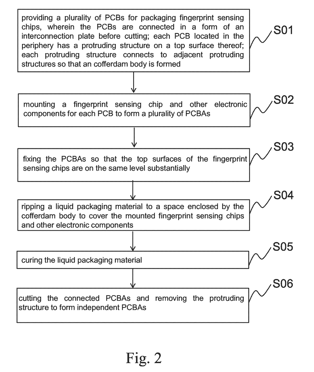
[0025]Please refer to FIG. 2. It is a flow chart of a method for packaging fingerprint sensing chips disclosed in the present invention. The method includes several steps. In order to have a comprehensive understanding of the spirit of the present invention, please refer to figures from FIG. 3 to FIG. 9 synchronously.

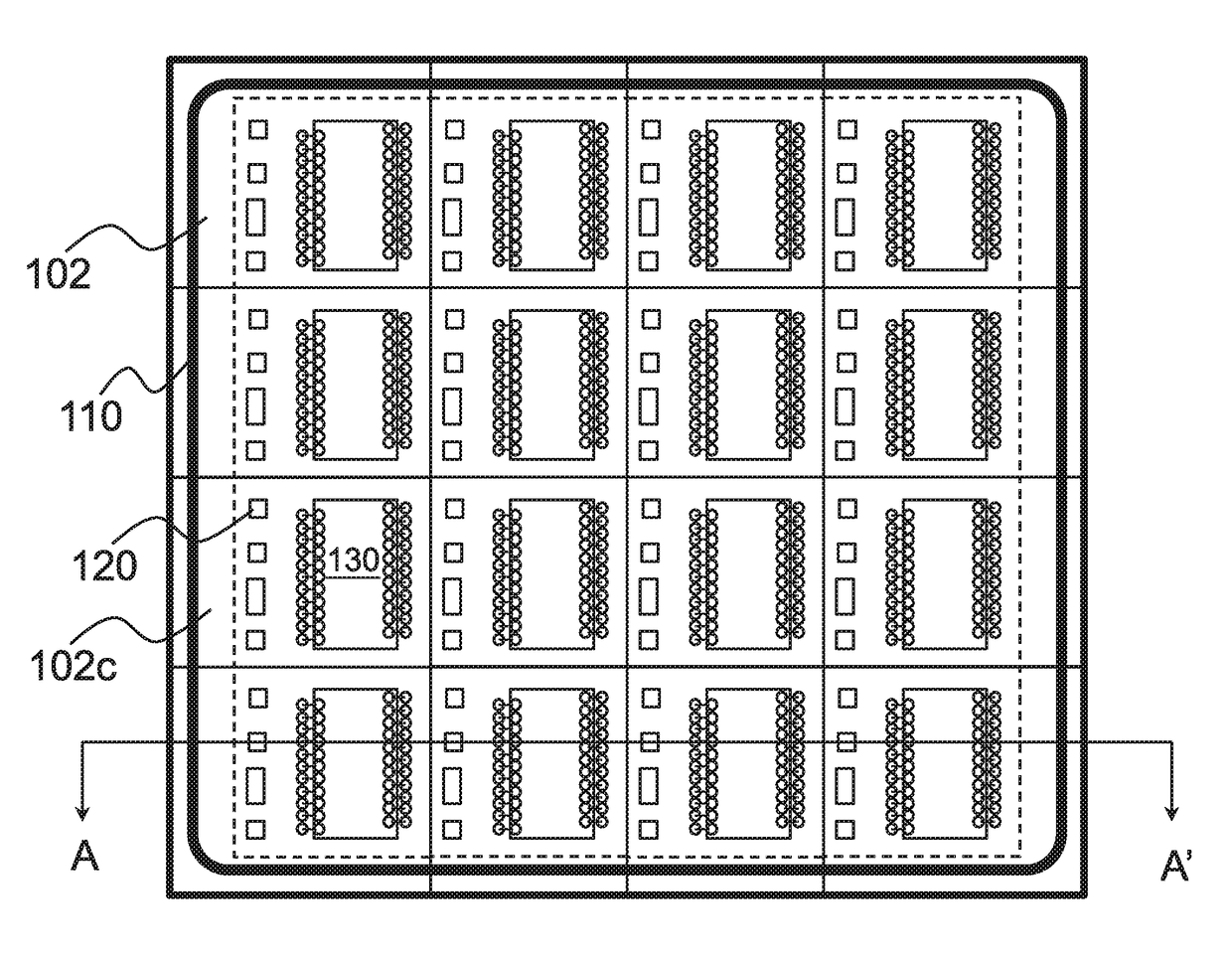
[0026]A first step of the present method is to provide a number of PCBs 100 for packaging fingerprint sensing chips 130. The PCBs 100 are connected in the form of a panel. Each PCB 100 located in the periphery has a protruding structure on its top surface, and protruding structure is perpendicular to the top surface. The protruding structure is similar to a dam bar structure. Each protruding structure connects to adjacent protruding structures so that a cofferdam body 110 is formed (S01). Please see FIG. 3. It is a top view of 16 PCBs forming a panel. As to te...


PUM


Abstract

A method for packaging fingerprint sensing chips and a fingerprint sensing module using the method are disclosed. The method includes the steps of: A. providing a number of PCBs for packaging fingerprint sensing chips, wherein the PCBs are connected in a form of a panel before cutting; each PCB located in the periphery has a protruding structure on a top surface thereof; each protruding structure connects to adjacent protruding structures to form an cofferdam body; B. mounting a fingerprint sensing chip and other electronic components for each PCB to form a number of PCBAs; C. fixing the PCBAs so that the top surfaces of the fingerprint sensing chips are on the same level substantially; D. dispensing a liquid packaging material to a space enclosed by the cofferdam body; E. curing the liquid packaging material; and F. cutting the connected PCBAs and removing the protruding structure to form independent PCBAs.

Description

FIELD OF THE INVENTION[0001]The present invention relates to a method for packaging fingerprint sensing chips and a fingerprint sensing module made by the method. More particularly, the present invention relates to a method for packaging fingerprint sensing chips using packaging material containing curable compositions and a fingerprint sensing module made by the method.BACKGROUND OF THE INVENTION[0002]Fingerprint sensing chip is the core element the devices utilizing fingerprints for security maintenance and identity verification. With blooming applications of mobile payment service on smartphones, the fingerprint sensing chip gradually becomes a necessary element of smartphones. Therefore, in order to fulfill the requirement of compact designs for smartphones, packaging method of fingerprint sensing chips which affects the size of the final product becomes more and more important. In addition, the packaging method is also a key factor affecting the appearance and performance of th...

Claims


Application Information

Patent Timeline
Patent Type & Authority Applications(United States)
IPC IPC(8): G06K9/00H01L23/00G06F21/32H04M1/667H04L9/32
CPCG06K9/00087H04M1/667H01L2224/02G06F21/32H01L24/08H04L9/3231H01L2924/181H01L21/561H01L24/32H01L24/48H01L24/49H01L24/73H01L24/97H01L2224/29339H01L2224/32225H01L2224/48091H01L2224/48227H01L2224/49175H01L2224/73265H01L2224/83801H01L2224/92247H01L2924/00014H01L2924/19105H01L23/3121G06V40/1329H01L2924/00012H01L2224/45099H01L2924/00G06V40/1365
Inventor HSIEH, CHUNG HAOHE, ZHENG PINGLIN, CHI CHOU
Owner SUNASIC TECH
Why Eureka
Try Eureka