High power LED array

Inactive Publication Date: 2006-03-09
OPTO TECH
View PDF3 Cites 48 Cited by
  • Summary
  • Abstract
  • Description
  • Claims
  • Application Information

AI Technical Summary

Benefits of technology

[0010] It is therefore an objective of the present invention to provide a high-power LE

Problems solved by technology

However, several drawbacks arise for the conventional high-power LED array.
First, when the high-power LED array is manufactured by assembling packed LEDs, the size of the LED array is usually bulky.
Additional assembling procedures are required, and the manufacturing cost is therefore increased.
Besides, optical misalignment is another issue concerned for the conventional high-power LED array.
The optical misalignment results from the misalignment of the packed LED during the assembling procedures.
Th

Method used


Image

  • High power LED array
  • High power LED array
  • High power LED array

Examples


Embodiment Construction

[0024] Reference will now be made in detail to the present preferred embodiments of the invention, examples of which are illustrated in the accompanying drawings. Wherever possible, the same reference numbers are used in the drawings and the description to refer to the same or like parts.

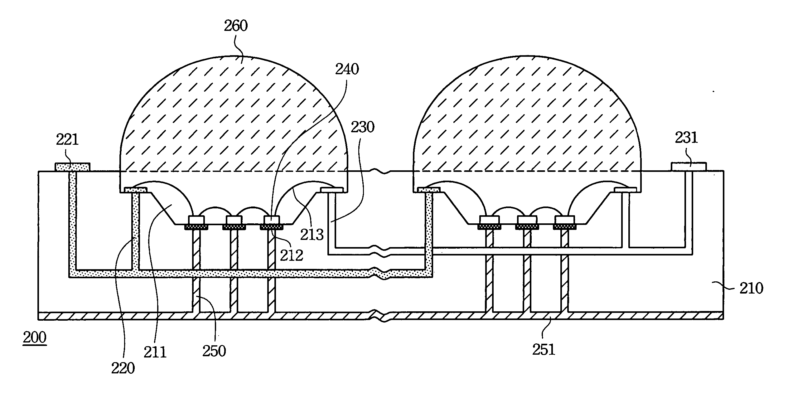
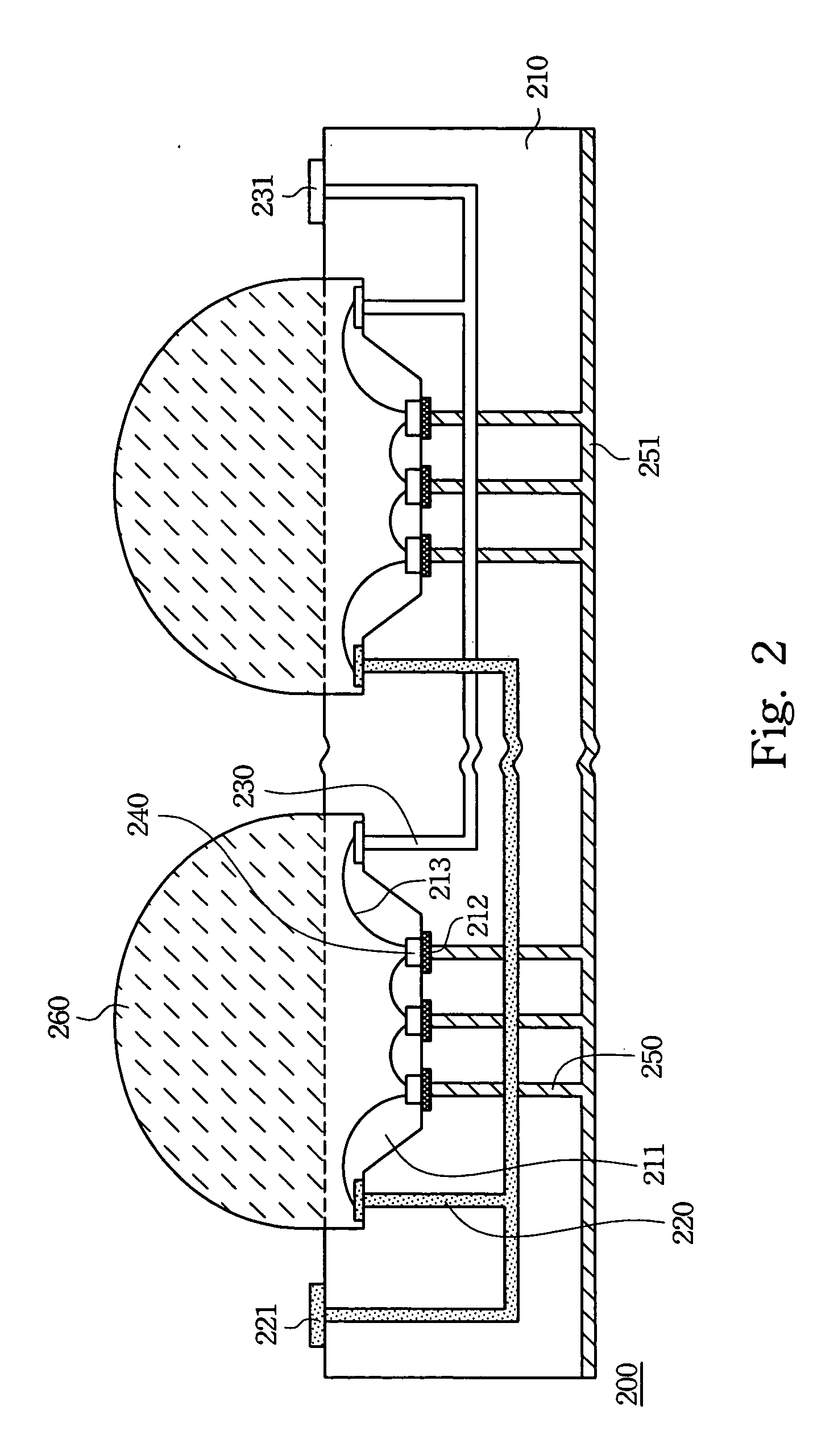
[0025] According to the high-power LED array of the present invention, the high-power LED dies are directly packed in the cavities of the PCB. The size of the high-power LED array can therefore be reduced dramatically. Further, the heat sink in the PCB also improves the efficiency of heat dissipation. Additionally, the placement of the lens on each cavity can be adjusted to optimize light output from the high-power LED array.

[0026]FIG. 2 is a cross-sectional diagram illustrating the high-power LED array according to the first preferred embodiment of the present invention. The high-power LED array 200 according to the first preferred embodiment of the present invention includes a PCB 210, anodes 22...


PUM


Abstract

The present invention relates to a high-power LED array. The high-power LED array has a printed circuit board (PCB), anodes, cathodes, high-power LED dies, packing materials, and lenses. The PCB has cavities arranged in an array. One anode and one cathode are located in each cavity. The anode and the cathode are correspondingly connected to the anode and cathode in the neighboring cavities. At least one high-power LED die is placed in the cavity and connected to the anode and the cathode in series or in parallel. The cavity is filled with packing material to secure the high-power LED die. Lenses are placed on the cavities to focus light emitted by the high-power LED die.

Description

RELATED APPLICATIONS [0001] The present application is based on, and claims priority from, Taiwan Application Serial Number 93127017, filed Sep. 7, 2004, the disclosure of which is hereby incorporated by reference herein in its entirety. BACKGROUND [0002] 1. Field of Invention [0003] The present invention relates a high-power Light Emitting Diode (LED). More particularly, the present invention relates to a high-power LED array. [0004] 2. Description of Related Art [0005] A high-power LED array, such as a III-V high-power LED array, is frequently employed in outdoor display panels. Conventionally, packed high-power LEDs are assembled on a Printed Circuit Board (PCB) to form this type of high-power LED array. FIG. 1 is a diagram illustrating the conventional high-power LED array. The high-power LED 100 includes an anode 101, a cathode 102, a high-power LED die 103, and a lens 104. The packed high-power LED 100 is connected to a PCB 110. [0006] The high-power LED die 103 is placed in a...

Claims


Application Information

Patent Timeline
IPC IPC(8): H01L31/0232H01L25/075H01L33/00
CPCH01L25/0753H01L2224/48091H01L2224/48137H01L2224/73265H01L2924/00014H01L2924/00
Inventor WANG, HUNG-TUNGHUNG, CHIEN-CHENTU, SHUN-LIHYEN, DENNIS CHIH-YUANCHUANG, CHIH-HUNGCHUNG, HUAI-KUYANG, CHENG-WEIHAN, TSU-AN
Owner OPTO TECH
Why Eureka
Try Eureka