Method of selective silicon nitride etching

a silicon nitride etching and selective technology, applied in the direction of basic electric elements, semiconductor/solid-state device manufacturing, electric apparatus, etc., can solve the problems of high aspect ratio, difficult control of current fluorocarbon chemistry used for sin etching,

Active Publication Date: 2017-11-30
TOKYO ELECTRON LTD
View PDF3 Cites 231 Cited by
  • Summary
  • Abstract
  • Description
  • Claims
  • Application Information

AI Technical Summary

Problems solved by technology

Next generation semiconductor technology development poses a huge challenge as dry etch removal of silicon nitride (SiN) selective to silicon oxide (SiO2) and other materials is needed.
Current fluorocarbon chemistry used for SiN etch becomes extremely difficult to control at narrow mask openings and high aspect ratio due to possibility of clogging of recessed features.

Method used


Image

  • Method of selective silicon nitride etching
  • Method of selective silicon nitride etching
  • Method of selective silicon nitride etching

Examples


Embodiment Construction

[0018]Embodiments of the invention describe substrate processing methods using non-polymerizing chemistry to selectively etch silicon nitride relative to other materials.

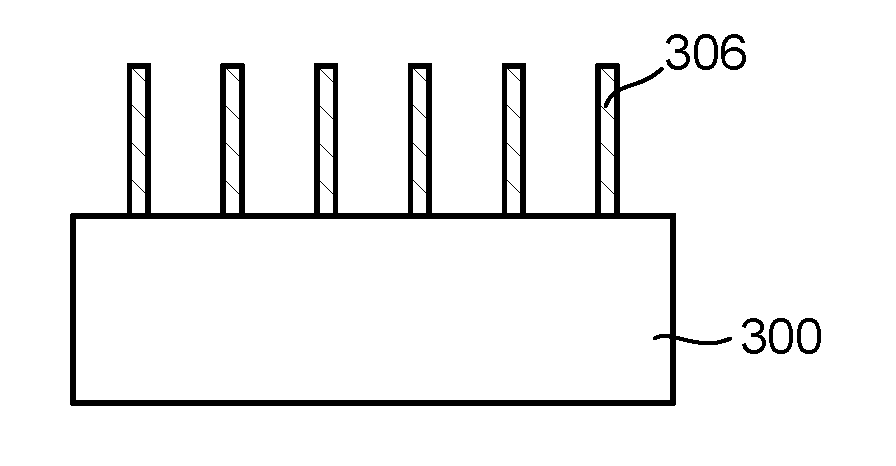
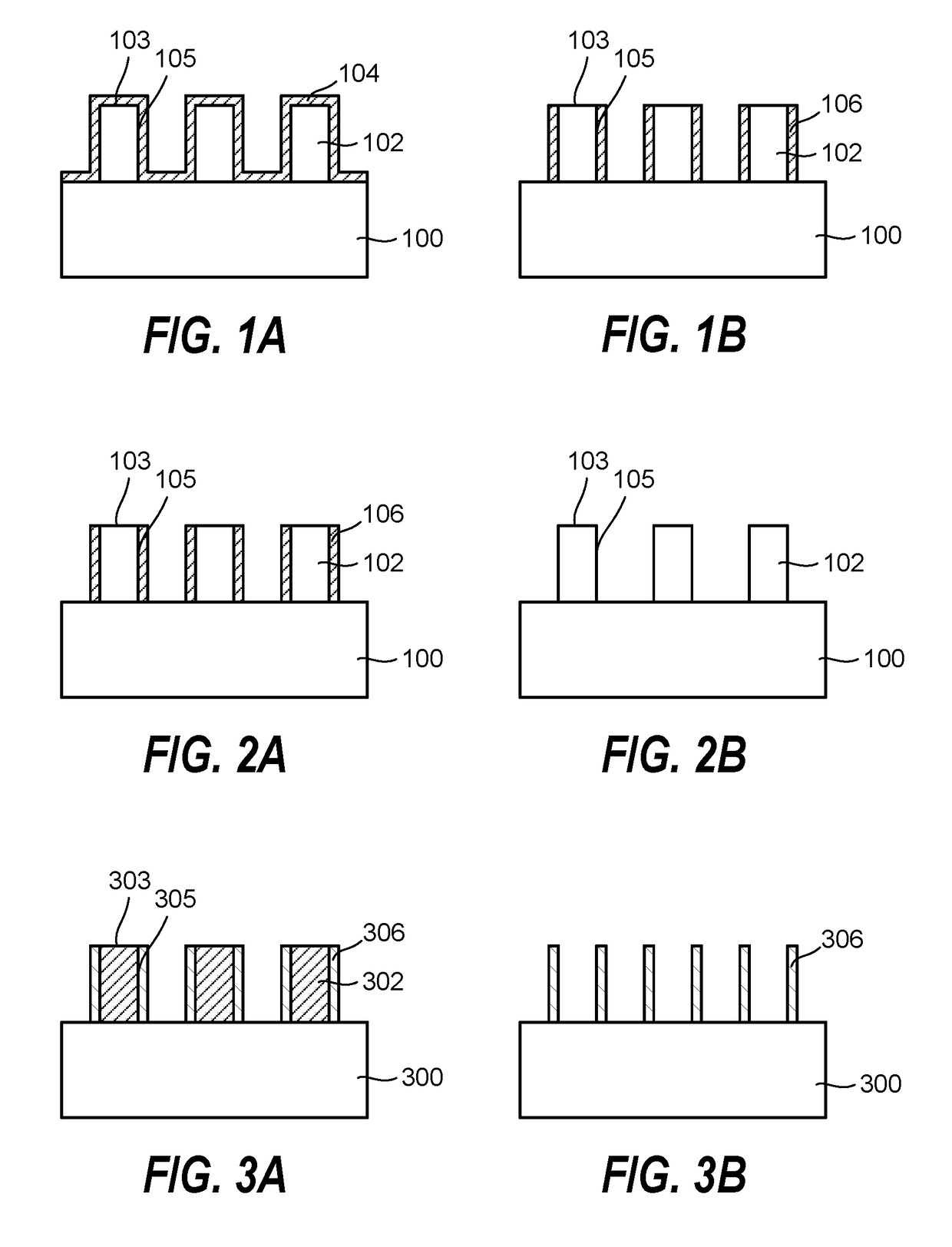
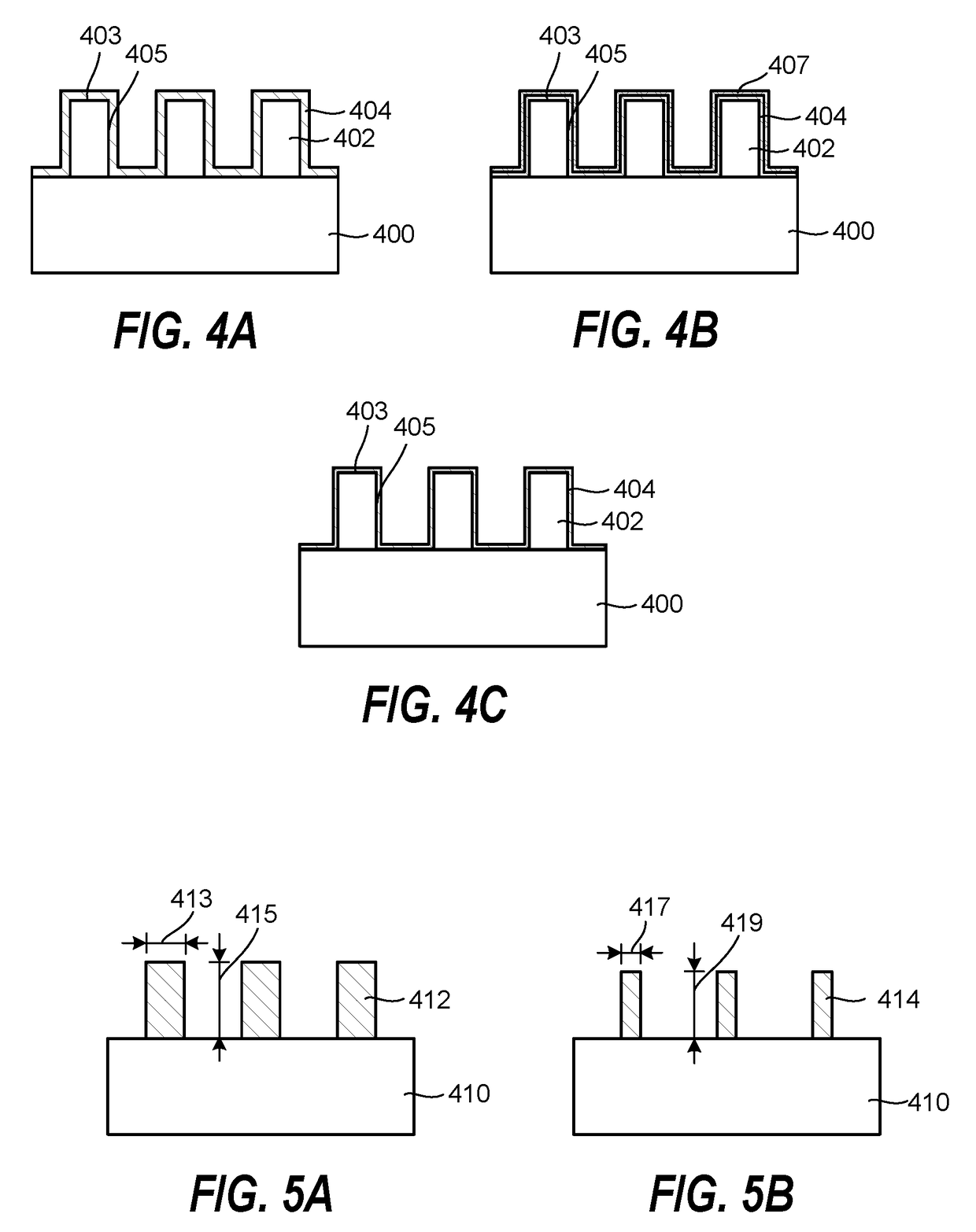
[0019]FIGS. 1A and 1B schematically show through cross-sectional views a method of processing a substrate according to an embodiment of the invention. FIG. 1A shows a substrate 100, raised features 102 on the substrate 100, and a SiN spacer layer 104 conformally formed on the exposed surfaces of the raised features 102 and the substrate 100. The exposed surfaces of the raised features 102 include vertical portions 105 and horizontal portions 103.

[0020]The substrate 100 and the raised features 102 may be selected from the group consisting of Si, SiO2, and a combination thereof. In some microelectronic devices, the raised features 102 are referred to as fins. As used herein, the notation “SiN” includes layers that contain silicon and nitrogen as the major constituents, where the layers can have a range of Si and N com...


PUM

PropertyMeasurementUnit
gas pressureaaaaaaaaaa
RF poweraaaaaaaaaa
frequencyaaaaaaaaaa

Abstract

Embodiments of the invention provide a substrate processing method for selective SiN etching relative to other layers used in semiconductor manufacturing. According to one embodiment, the substrate processing method includes providing in a plasma processing chamber a substrate containing a first material containing silicon nitride and a second material that is different from the first material, forming a plasma-excited process gas containing NF3 and O2, and exposing the substrate to the plasma-excited process gas to selectively etch the first material relative to the second material. According to one embodiment, the second material may be selected from the group consisting of Si, SiO2, and a combination thereof.

Description

CROSS-REFERENCE TO RELATED APPLICATIONS[0001]This application is related to and claims priority to U.S. Provisional Patent Application Ser. No. 62 / 342,991 filed on May 29, 2016, the entire contents of which are herein incorporated by reference. This application is related to and claims priority to U.S. Provisional Patent Application Ser. No. 62 / 384,481 filed on Sep. 7, 2016, the entire contents of which are herein incorporated by reference.FIELD OF INVENTION[0002]The present invention relates to the field of semiconductor manufacturing and semiconductor devices, and more particularly, to a method of selective silicon nitride etching relative to other materials used in semiconductor manufacturing.BACKGROUND OF THE INVENTION[0003]Next generation semiconductor technology development poses a huge challenge as dry etch removal of silicon nitride (SiN) selective to silicon oxide (SiO2) and other materials is needed. Current fluorocarbon chemistry used for SiN etch becomes extremely diffic...

Claims


Application Information

Patent Timeline
Patent Type & Authority Applications(United States)
IPC IPC(8): H01L21/311
CPCH01L21/31116H01L21/0217H01L21/02274H01L21/0228H01L21/0337H01L21/3065H01L21/32136H01L21/67069
Inventor RANJAN, ALOKRASTOGI, VINAYAKSHERPA, SONAM D.
Owner TOKYO ELECTRON LTD
Why Eureka
Try Eureka