

Techniques for fabricating horizontally aligned nanochannels for microfluidics and biosensors
a nanochannel and nanopore technology, applied in the field of nanochannel devices, can solve the problems of incompatibility with large-scale integration, device unsatisfactory from an application point of view, and difficult fabrication of nanochannels or nanopores with ultra-thin alternating layer properties (i.e., multi-layers of insulators/metals) in the nanoscale rang
- Summary
- Abstract
- Description
- Claims
- Application Information
AI Technical Summary
Benefits of technology
Problems solved by technology
Method used
Image

Examples
Embodiment Construction
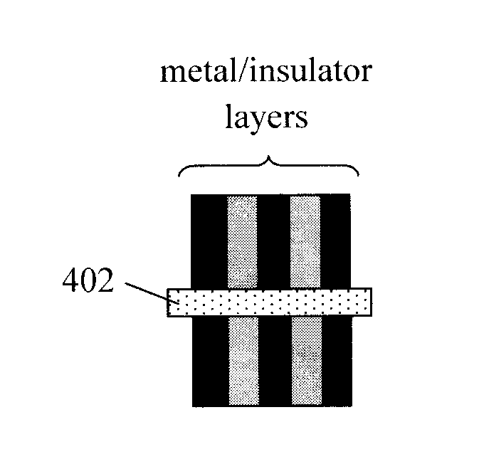
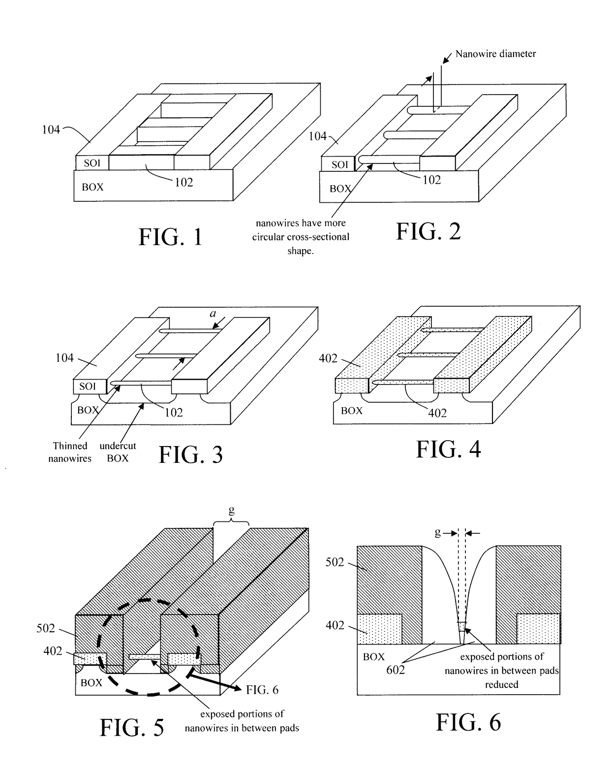
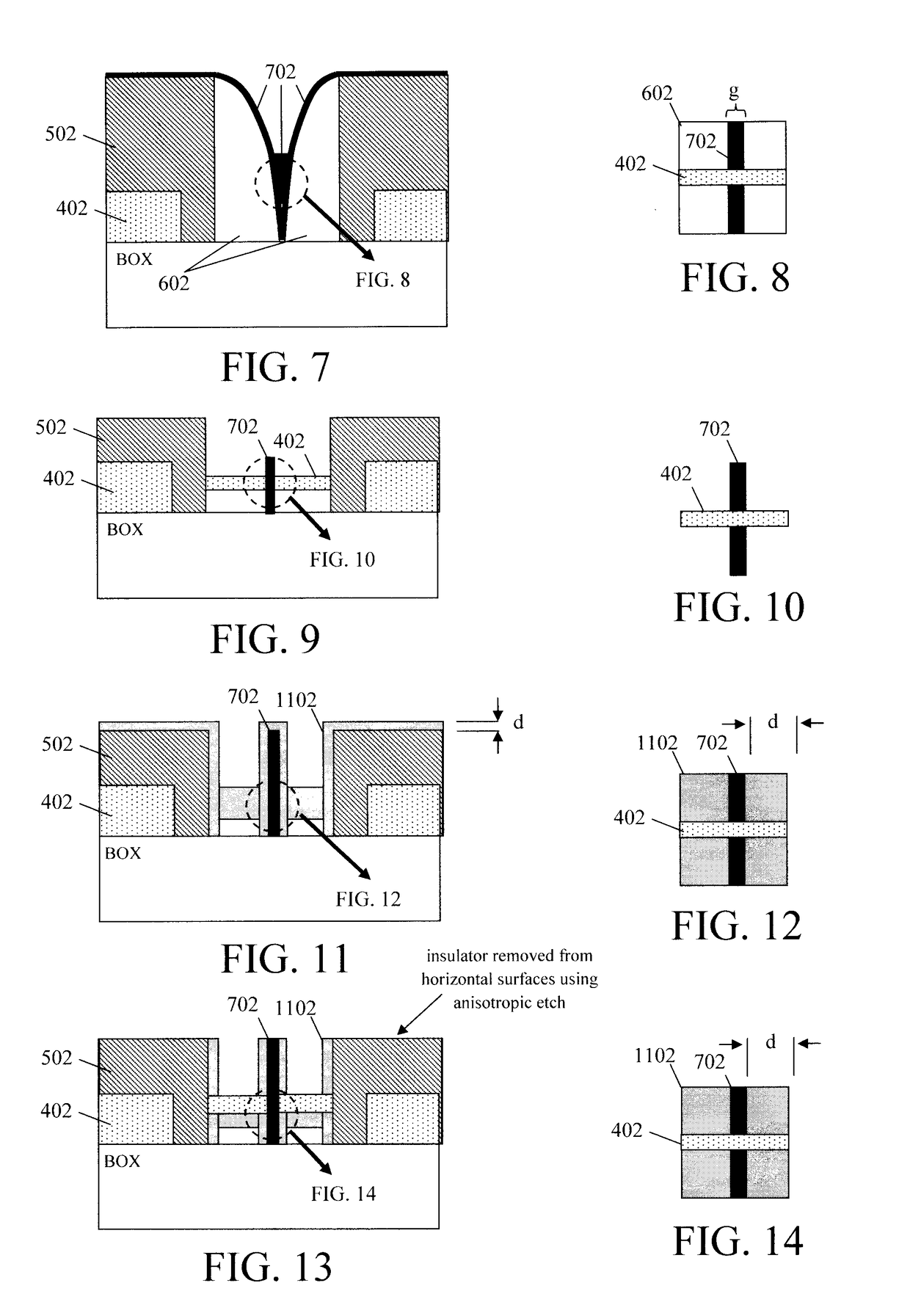
[0045]Provided herein are techniques for fabricating horizontally aligned nanochannels useful for a variety of applications. As will be described in detail below, the present techniques leverage the accessibility of a nanowire to recess a whole layer of thickness d from the nanowire, where etching on the extent of d / 2 occurs from 2 fronts. The same amount of etch has to be expected on the sidewall, leaving d / 2 of the original deposited thickness d on the sidewall. By repeating the above procedure, alternating layers of very fine thickness can be deposited around a dummy wire. The dummy wire can then be selectively removed to form the nanofluidic nanochannels.
[0046]A first exemplary embodiment of the present techniques are now described in detail by way of reference to FIGS. 1-26. As shown in FIG. 1, the process begins with a wafer in which at least one nanowire 102 has been defined. According to the exemplary embodiment shown illustrated in the figures, the starting wafer is a silic...
PUM
| Property | Measurement | Unit |
|---|---|---|
| distance | aaaaa | aaaaa |
| channel diameter | aaaaa | aaaaa |
| sizes | aaaaa | aaaaa |
Abstract
Description
Claims
Application Information