
Redistribution layer (RDL) fan-out wafer level packaging (FOWLP) structure

Inactive Publication Date: 2017-12-28
QUALCOMM INC
View PDF17 Cites 7 Cited by
  • Summary
  • Abstract
  • Description
  • Claims
  • Application Information

AI Technical Summary

Benefits of technology

The patent is about a new method of packaging semiconductor devices called FOWLP, which allows for more connections and better performance compared to standard WLP. This is done by embedding individual semiconductor devices in a low-cost material and allocating space between them for additional connections. The method allows for the connections to fan-out from the semiconductor device's footprint on the wafer. The patent includes a computer-readable medium that describes a process for designing a semiconductor die with at least one input / output connection. The process includes providing a first plurality of package balls with a first layout, forming a first conductive layer to connect to the package balls, and forming a second conductive layer with at least one conductive pillar to connect to the semiconductor die's input / output connection. This allows the semiconductor die to be connected to a second plurality of package balls without changing their position.

Problems solved by technology

Using this method, there is a limit to the number of I / O connections that a given semiconductor device can have.

Method used


Image

  • Redistribution layer (RDL) fan-out wafer level packaging (FOWLP) structure
  • Redistribution layer (RDL) fan-out wafer level packaging (FOWLP) structure
  • Redistribution layer (RDL) fan-out wafer level packaging (FOWLP) structure

Examples


Embodiment Construction

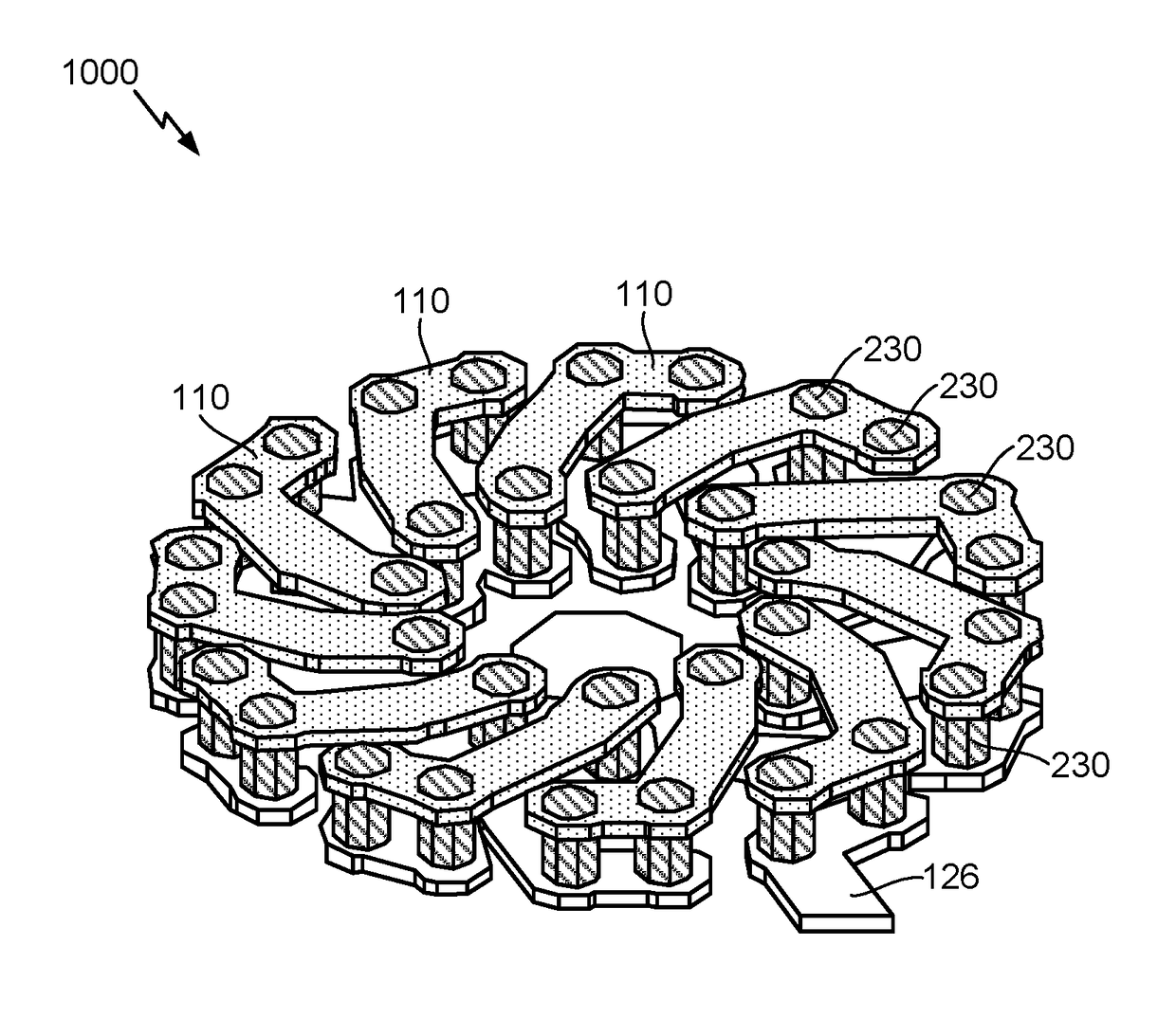
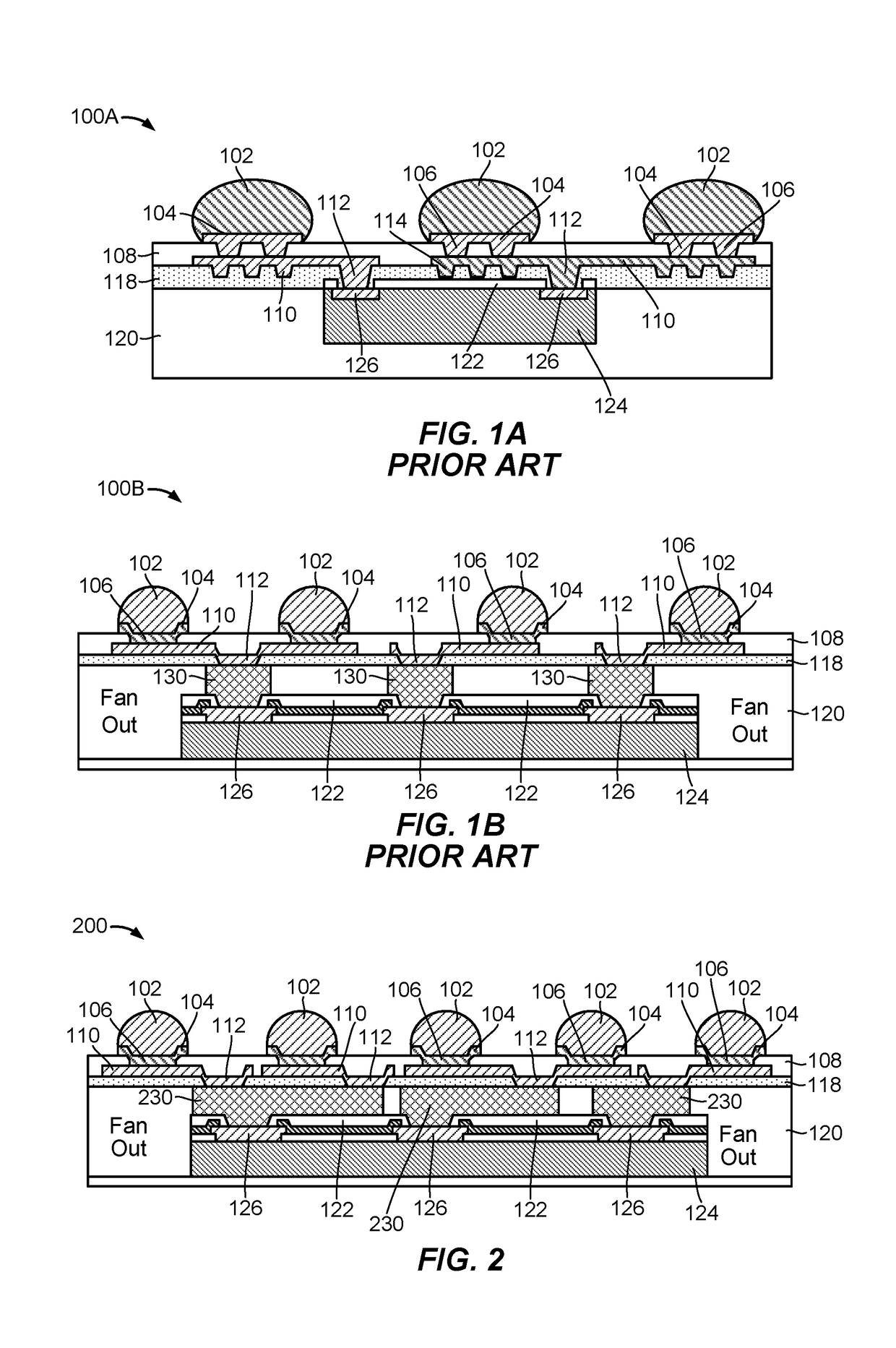
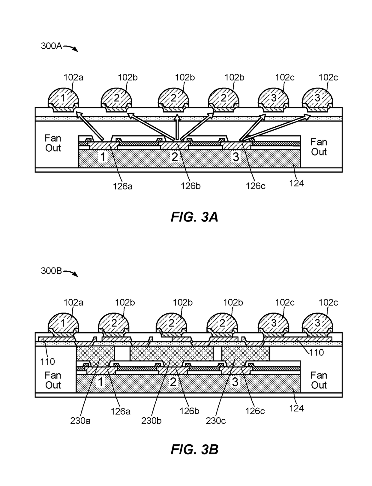
[0026]Disclosed is a fan-out wafer level packaging (FOWLP) apparatus that includes a semiconductor die having at least one input / output (I / O) connection, a first plurality of package balls having a first package ball layout, a first conductive layer forming a first redistribution layer (RDL) and configured to electrically couple to the first plurality of package balls, and a second conductive layer forming a second RDL and including at least one conductive pillar configured to electrically couple the at least one I / O connection of the semiconductor die to the first conductive layer, wherein the second conductive layer enables the semiconductor die to be electrically coupled to a second plurality of package balls having a second package ball layout without a change in position of the at least one I / O connection of the semiconductor die.

[0027]These and other aspects of the disclosure are disclosed in the following description and related drawings directed to specific embodiments of th...


PUM


Abstract

Disclosed is a fan-out wafer level packaging (FOWLP) apparatus includes a semiconductor die having at least one input / output (I / O) connection, a first plurality of package balls having a first package ball layout, a first conductive layer forming a first redistribution layer (RDL) and configured to electrically couple to the first plurality of package balls, and a second conductive layer forming a second RDL and including at least one conductive pillar configured to electrically couple the at least one I / O connection of the semiconductor die to the first conductive layer, wherein the second conductive layer enables the semiconductor die to be electrically coupled to a second plurality of package balls having a second package ball layout without a change in position of the at least one I / O connection of the semiconductor die.

Description

INTRODUCTION[0001]Embodiments relate to a redistribution layer (RDL) fan-out wafer level packaging (FOWLP) structure.[0002]FOWLP is an enhancement of standard wafer-level packaging (WLP) developed to provide a solution for semiconductor devices requiring a higher integration level and a greater number of external contacts. It also provides a smaller package footprint with higher input / output (I / O), along with better thermal and electrical performance than standard WLP.[0003]Specifically, in conventional WLP (also referred to as “fan-in” WLP), I / O terminals can only be located within the footprint of the semiconductor device on the wafer. Using this method, there is a limit to the number of I / O connections that a given semiconductor device can have. In contrast, FOWLP takes individual semiconductor devices and embeds them in a low cost material, such as epoxy mold compound (EMC), with space allocated between each semiconductor device for additional I / O connection points. In this way,...

Claims


Application Information

Patent Timeline
IPC IPC(8): H01L23/00H01L23/31H01L23/498
CPCH01L24/14H01L2224/02373H01L2224/02379H01L2224/13024H01L2224/1412H01L2224/13147H01L2924/141H01L2924/19011H01L2924/19042H01L2924/2064H01L2224/13124H01L2224/13111H01L2224/13155H01L2224/13139H01L2224/13144H01L2224/13116H01L2224/13113H01L2924/1431H01L2924/1433H01L2924/14335H01L23/49822H01L2224/14177H01L2224/02372H01L23/49838H01L2224/1416H01L2224/02331H01L23/3114H01L2224/14131H01L2224/0233H01L23/3128H01L21/561H01L24/02H01L24/05H01L24/06H01L24/13H01L24/96H01L2224/0235H01L2224/02375H01L2224/02381H01L2224/04105H01L2224/05111H01L2224/05124H01L2224/05139H01L2224/05144H01L2224/05147H01L2224/05155H01L2224/06131H01L2224/12105H01L2224/96H01L2224/05569H01L2224/05572H01L2924/381H01L23/5227H01L23/5389H01L2224/03H01L2224/11
Inventor OH, JIHOONZANG, RUEY KAEKESER, LIZABETH ANNALVARADO, REYNANTE TAMUNANXU, HAIYONGLI, YUEBEZUK, STEVE
Owner QUALCOMM INC
Learn More