
Organic light emitting diode display

a light-emitting diode display and organic technology, applied in the direction of cathode-ray tube indicators, static indicating devices, instruments, etc., can solve the problems of image sticking, reduce the lifetime of the organic light-emitting display panel, etc., to reduce power consumption, reduce flicker phenomenon, and suppress luminance drop

Active Publication Date: 2018-01-04
LG DISPLAY CO LTD
View PDF8 Cites 6 Cited by
  • Summary
  • Abstract
  • Description
  • Claims
  • Application Information

AI Technical Summary

Benefits of technology

The present disclosure relates to reducing power consumption and flicker in an organic light emitting display. By driving the display at a low rate, and using an internal or external voltage compensation method in each pixel, the inventors have been able to decrease the luminance during the refresh period. This has resulted in a better image quality and reduced flickering on the display. Additionally, the use of a distributed gate signaling during a plurality of refresh periods further reduces luminance decrease and flickering.

Problems solved by technology

Also, a characteristic difference caused by deterioration of the driving TFT occurring while the organic light emitting diode is driven may reduce the lifetime of an organic light emitting display panel or cause image sticking.

Method used


Image

  • Organic light emitting diode display
  • Organic light emitting diode display
  • Organic light emitting diode display

Examples


example 1

Structure

[0148]FIG. 11 is a circuit diagram showing a pixel circuit 1000 in an OLED device according to still another exemplary embodiment of the present disclosure. FIG. 12 is a waveform diagram showing a signal input into the pixel circuit 1000 illustrated in FIG. 11 and a resultant output signal. A signal input into a pixel circuit 1000 illustrated in FIG. 12 may be substantially the same as the signal input into the pixel circuit 800 illustrated in FIG. 9, except for certain aspects. Therefore, a redundant explanation thereof will be omitted or brief herein. The pixel circuit 1000 illustrated in FIG. 11 is substantially the same as the pixel circuit 800 illustrated in FIG. 9 except for certain aspects such as that a fourth switching TFT T4 is further provided. Therefore, a redundant explanation thereof will be omitted or brief herein.

[0149]Referring to FIG. 11, the pixel circuit 1000 includes the driving TFT DT, four switching TFTs, and two capacitors.

[0150]The fourth switching ...

example 2

-Added Structure

[0167]Hereinafter, a pixel of the present disclosure will be described in detail. FIG. 14 is a driving circuit diagram of the pixel illustrated in FIG. 1.

[0168]Referring to FIG. 14, a pixel 1 includes an organic light emitting diode OLED and a pixel driving circuit 200 including four transistors and three capacitors and configured to drive the organic light emitting diode OLED.

[0169]Specifically, the pixel driving circuit 200 includes a driving transistor DT, first to third switching transistor T1 to T3, and first to third capacitors C1 to C3.

[0170]In this case, the first capacitor C1 and the second capacitor C2 may be storage capacitors and the third capacitor C3 may be a coupling capacitor.

[0171]The driving TFT DT includes a gate node as a first node N1 connected to the first switching TFT T1, a source node as a second node N2 connected to the second switching TFT T2, and a drain node connected to the third switching TFT T3.

[0172]Specifically, the gate node of the ...


PUM


Abstract

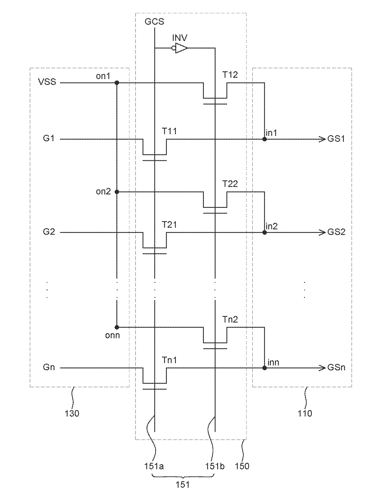
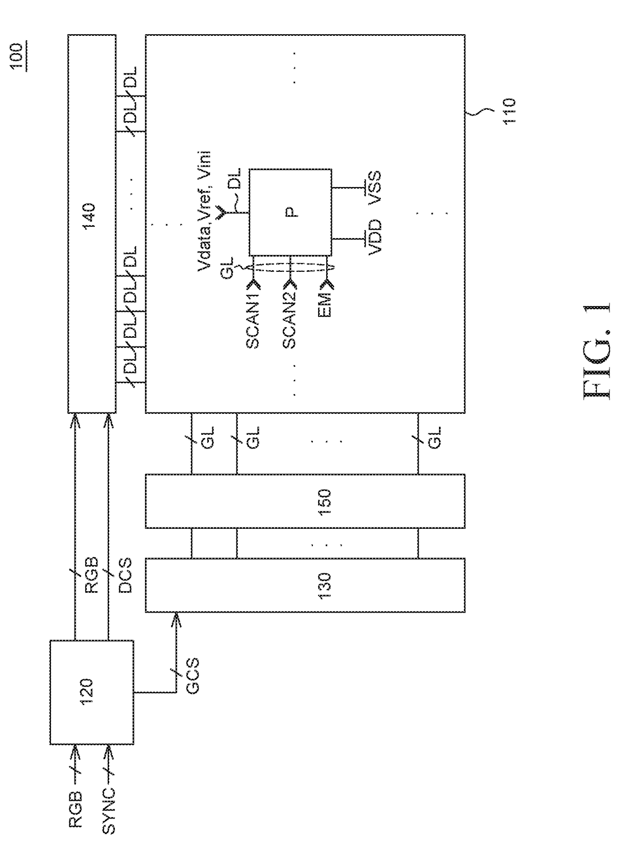
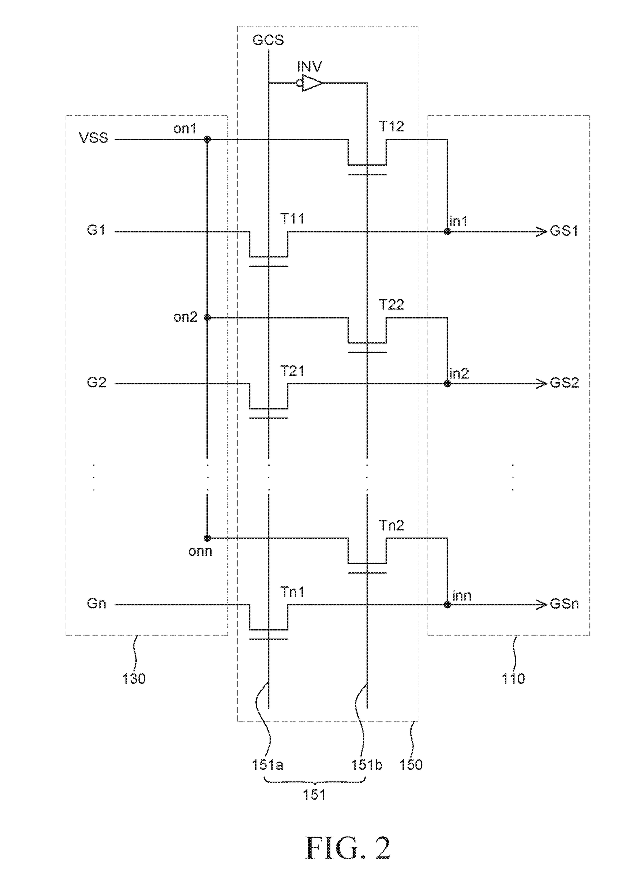
Provided is an organic light emitting display. The organic light emitting display can include a gate driving circuit configured to supply a gate signal through each of a plurality of gate lines connected to a display panel, and a luminance control unit between the gate driving circuit and the display panel and electrically connected to the plurality of gate lines and a power supply line. A gate signal is supplied to the pixels in a distributed manner during a plurality of refresh periods. Therefore, it is possible to reduce a luminance decrease in the pixels during the entire refresh period.

Description

CROSS-REFERENCE TO RELATED APPLICATIONS[0001]This application claims the priority of Korean Patent Application No. 10-2016-0083057 filed on Jun. 30, 2016 and Korean Patent Application No. 10-2016-0178133 filed on Dec. 23, 2016, in the Korean Intellectual Property Office, the disclosures of all of which are incorporated herein by reference.BACKGROUNDField[0002]The present disclosure relates to an organic light emitting diode display, and more particularly, to an organic light emitting display capable of suppressing a flicker phenomenon.Description of the Related Art[0003]Recently, as information technology has developed, various display devices with excellent performance, such as thinning, weight lightening, and low power consumption, have been developed.[0004]Specific examples of the display devices include a Liquid Crystal Display (LCD) device, a Field Emission Display (FED) device, an Organic Light Emitting Display (OLED) device, and the like.[0005]Each of a plurality of pixels co...

Claims


Application Information

Patent Timeline
Patent Type & Authority Applications(United States)
IPC IPC(8): G09G5/10G09G3/3233G09G3/3266
CPCG09G5/10G09G3/3266G09G2330/021G09G2310/061G09G2320/0247G09G3/3233G09G2300/0819G09G2300/0852G09G2300/0861G09G2310/0251G09G2310/0262G09G2320/043
Inventor KIM, KITAECHOI, SEUNGCHANLEE, JUNHORYU, SUNGBINYOON, SIU
Owner LG DISPLAY CO LTD
Learn More